DC-DC buck converters are essential for efficiently powering subsystems in automotive, industrial, and consumer electronics. While selecting the right regulator is critical, the PCB layout ultimately determines whether the converter performs as intended.
A well-optimized design can prevent many common issues, whereas a poor layout often leads to problems—especially at high current levels and large input-to-output voltage differentials.
By following fundamental layout guidelines, these issues can be minimized, ensuring reliable and efficient power delivery. `
Why PCB Layout is Critical in DC-DC buck converter Design?
The PCB layout directly influences:
Power efficiency
Power efficiency in a buck converter is not only determined by the silicon and switching strategy but is heavily influenced by PCB layout, particularly trace resistance and thermal design.
Current-carrying paths such as input-to-FET, FET-to-inductor, and inductor-to-output must be kept short and wide to reduce I²R losses.
For example, a 50 mil wide, 1oz copper trace carrying 8A could dissipate over 0.5W over just a few centimeters—wasting power and generating heat.
This heat build-up increases junction temperature and may reduce efficiency further through increased Rdson of FETs and ESR of capacitors.
Proper thermal via placement under hot components and large copper pours are essential for minimizing these losses and maintaining high conversion efficiency, particularly under full load.
Also Read: How to Select a TVS Diode to Suppress Transients in Electrical Circuits?
Noise and EMI
The high-frequency switching action of buck converters generates significant noise that can propagate through both conduction and radiation, potentially disrupting sensitive electronics and failing regulatory tests.
The primary sources of EMI in these circuits include the switching node (SW), input ripple currents, and ground bounce effects, each requiring specific mitigation strategies.
For instance, the SW node acts as a potent source of radiated magnetic fields due to its high dv/dt characteristics, which can be addressed through careful loop area minimization, shielding techniques, and RC snubber networks.
Similarly, conducted noise on the input power rail demands low-ESR ceramic capacitors and pi-filter topologies to attenuate high-frequency harmonics before they reach other system components.
Ground bounce—a common issue in high-current designs—arises from shared return path impedance and can be mitigated through star grounding configurations and dense via stitching to maintain low-impedance return paths.
EMI performance is critically tied to how the PCB layout handles parasitic elements and high-frequency current loops. Fast switching edges on the SW node generate high dv/dt and di/dt, which can cause ringing and radiated noise if loop areas are large or poorly shielded.
Key radiating loops—especially the input loop (VIN → High-side FET → Low-side FET → CIN return)—should be minimized in area and enclosed by a solid ground plane. Routing the noisy SW node over long traces or near analog circuitry results in capacitive coupling that injects noise into adjacent nets.
Parasitic inductance in power paths also leads to overshoot and ringing, increasing conducted EMI. Proper decoupling, shielded inductors, snubbers, and compact current loops are essential layout tactics to mitigate both radiated and conducted noise.
Designers must minimize this loop area to reduce parasitic inductance, which would otherwise generate voltage spikes (V = L·di/dt) that exacerbate EMI. Practical implementation involves using wide copper pours for high-current traces, placing low-ESL (equivalent series inductance) capacitors as close as possible to switching elements, and ensuring the ground return path is direct and low-impedance.
Regulator stability
The stability of a buck converter’s control loop hinges on clean, noise-free feedback and proper placement of compensation networks. Improper feedback routing—especially if the FB line is routed near the noisy SW node or power traces—can inject switching noise into the regulation loop, causing jitter, subharmonic oscillation, or even outright instability.
Kelvin sensing directly from the output capacitor terminals (rather than from the inductor or remote locations) ensures accurate regulation. Compensation components (RC networks) should be placed close to the controller IC and routed away from EMI sources.
In high-speed or high-current applications, differential feedback routing may be necessary for long feedback paths to maintain signal integrity. A stable loop not only ensures accurate DC regulation but also impacts transient response and EMI behavior.
Thermal Performance in DC-DC Buck Converter Design
Thermal management is a critical aspect of DC-DC buck converter design, especially in high-temperature environments such as automotive or industrial applications where ambient temperatures can exceed 125°C. Even the most efficient electrical design can suffer from performance degradation or failure if thermal considerations are overlooked.
The primary factors influencing thermal performance include copper thickness, board layout, and stackup configuration. Using 2oz copper instead of the standard 1oz significantly improves heat dissipation, as the thicker copper layers provide lower thermal resistance and better current-carrying capacity.
Additionally, proper utilization of exposed pads with via arrays is essential for transferring heat from power components into the inner layers of the PCB, where it can be spread more effectively. A well-designed board stackup, particularly one with four or more layers incorporating dedicated ground and power planes, further enhances thermal spreading by providing additional pathways for heat to dissipate.
Practical thermal strategies are essential to ensure reliable operation under high-load conditions. For instance, in a 12V/8A buck converter, even a modest 5mΩ resistance in the power path results in a 0.32W power loss, which can create localized hotspots if not properly managed.
These hotspots can lead to premature component failure or unexpected thermal throttling. To mitigate these risks, designers should employ thermal imaging during the prototyping phase to identify areas of poor thermal flow and optimize the layout accordingly.
Following IPC-2152 guidelines for trace widths and thermal via placement is also crucial, as these standards provide empirically validated recommendations for managing heat dissipation in high-current applications.
By integrating these thermal strategies early in the design process, engineers can ensure that their buck converters operate reliably even under the most demanding conditions, balancing electrical performance with thermal efficiency.
✅ Key PCB Layout Design Consideration of DC-DC Buck Converters
Bypass Capacitor
Effective use of bypass capacitors is critical for minimizing high-frequency noise and maintaining power integrity in high-speed circuits. To optimize their performance, the bypass loop inductance must be minimized.
This is achieved by reducing the physical loop area—especially in high di/dt (current slew rate) paths—through short, direct trace lengths, low-inductance ground planes, and routing current directly across the capacitor terminals.
Avoid routing across multiple planes or using unnecessary vias, which can increase impedance and degrade performance.
To achieve low impedance across a wide frequency band, designers should parallel capacitors of different dielectric types and values. For instance, combining 0.1 μF and 0.01 μF MLCCs effectively suppresses noise in the 2 MHz to 20 MHz range due to their complementary impedance characteristics.
Placing bypass capacitors as close as physically possible to the power pins of the integrated circuit (IC) is essential. This proximity not only improves decoupling efficiency but also visually identifies critical nodes and high-speed current return paths for layout designers, enabling better prioritization during PCB routing.
Load Current Capability
The converter’s rated load current dictates the sizing of PCB traces, copper pours, and thermal vias to prevent overheating and minimize voltage drops. High-current paths—typically between the input capacitor, FETs, inductor, and output capacitor—must be routed with wide, low-impedance copper tracks.
According to IPC-2152 standards, a 1oz copper trace carrying 8A requires at least 300 mil (7.6mm) width for surface layers, more if buried. Undersized traces not only lead to resistive losses but can also cause thermal runaway or hotspot formation. Therefore, the load current specification directly shapes both the electrical and thermal aspects of the PCB design.
Switching Frequency
Switching frequency in buck converters determines the size of passive components and affects overall power density. Higher frequencies (e.g., >1MHz) allow for smaller inductors and capacitors, enabling compact designs ideal for handheld or automotive applications.
However, increasing frequency also exacerbates EMI emissions due to faster voltage and current transitions (higher dv/dt and di/dt). This necessitates careful PCB layout with tight switching loops, shielded inductors, and filtering techniques like snubbers and ferrite beads.
Designers must strike a balance between frequency, efficiency, thermal stress, and EMI compliance, often selecting a mid-range frequency (400kHz–800kHz) for optimal trade-off.
Thermal Resistance (RθJA)
Thermal resistance, typically expressed as junction-to-ambient (RθJA), defines how effectively heat generated inside the IC is dissipated into the surrounding environment.
It is measured in °C/W, where a lower value indicates better thermal performance. For instance, an IC dissipating 1W of power with an RθJA of 50°C/W will experience a junction temperature rise of 50°C above ambient.
Factors affecting RθJA include the IC package type (e.g., QFN vs. D2PAK), exposed pad connectivity, copper area under the pad, and the number and placement of thermal vias.
High RθJA values can lead to thermal throttling or failure in high-current designs, making it crucial to optimize thermal paths during layout and to use techniques like copper pouring and heat sinking to manage heat effectively.
Feedback Compensation Network
For optimal control loop stability and noise immunity, the compensation network should be placed as close as possible to the IC’s error amplifier. Specifically, the feedback (FB) node—which connects to the inverting input of the error amplifier—must be routed with minimal trace length and minimal parasitic inductance or capacitance.
Place compensation resistors and capacitors directly adjacent to the FB pin, ensuring that the resistors form a tight connection between the FB node and the voltage divider or output sensing point. This minimizes potential noise pickup and ensures accurate voltage regulation by preserving the integrity of the sensed output signal.
Avoid long traces or routing through multiple layers for compensation components, as these can introduce unwanted delay, oscillation, or phase shift into the feedback loop.
FET Placement and Layout for High di/dt Paths
In power stage design, it is essential to carefully route high di/dt (current slew rate) paths, particularly around switching elements such as power MOSFETs and output capacitors. Improper layout can introduce parasitic inductance into the current loop, leading to switch-node ringing.
This ringing not only increases electromagnetic interference (EMI) and harmonic distortion but can also exceed the absolute maximum voltage ratings of switching FETs, potentially leading to device failure.
To mitigate these effects, the primary objective is to minimize the high-frequency loop area. This can be achieved by:
- Utilizing a compact layout with tight current loops, especially in the switch-node and input bypass paths.
- Routing power traces wide and short, and using multiple vias to reduce current path resistance and inductance.
- Ensuring that high-current return paths (e.g., ground) are routed in a way that mirrors the forward path, maintaining loop symmetry.
- With proper component placement and routing, the need for snubber networks to suppress switch-node ringing can often be eliminated, resulting in a more efficient and robust power design.
Managing Parasitic Components
Parasitic inductance and capacitance are inherent in PCB layouts and, if unmanaged, can degrade power supply performance by increasing impedance, introducing resonances, and compromising stability. These parasitics are especially problematic in low-impedance paths, such as power stages, filters, and timing-critical switching nodes.
- Minimize parasitic inductance by:
- Using continuous ground planes to reduce return path impedance.
- Routing wide, short traces—especially in high-current paths.
- Avoiding unnecessary vias in current loops and ensuring tight coupling between power and return paths.
- Paying special attention to wiring inductance in filter and feedback circuits.
- Control parasitic capacitance by:
- Minimizing stray coupling to high-impedance or noise-sensitive nodes (e.g., compensation networks, feedback lines).
- Managing interlayer spacing to reduce unwanted plane-to-plane capacitance.
- Reducing capacitive coupling to pads and sensitive signal traces by maintaining adequate spacing from high-speed nodes.
- Mitigate magnetic coupling by:
- Orienting inductors—particularly toroidal types—to avoid mutual flux linkage.
- Physically separating magnetics when possible, or rotating them to minimize field interaction.
- Reducing loop area in both signal and power paths to limit cross-coupling between adjacent current loops.
- Proper parasitic management not only improves EMI performance but also enhances regulation accuracy and transient response, contributing to a stable and noise-immune power delivery system.
Design Approach 1: External FET DC-DC Buck Converters
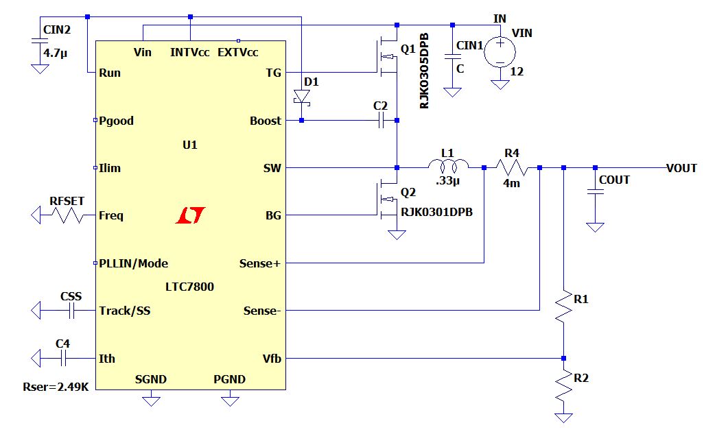
External FET DC-DC Buck Converter Schematic Example
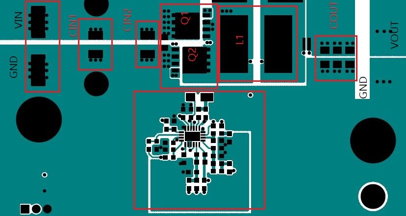
External FET DC-DC Buck Converter PCB Layout Example
✅ External FET DC-DC Buck Converter PCB Layout Checklist
Effective component placement is the foundation of a robust and efficient buck converter layout. Strategic positioning reduces parasitic effects, optimizes thermal management, and minimizes EMI susceptibility.
- Input capacitors (CIN) placed as close as possible to the high-side FET drain (VIN) and source to minimize input loop area.
- Use parallel combination of low-ESR ceramic capacitors (X7R, 10–22µF) and bulk electrolytic/tantalum capacitors for stable filtering.
- Keep VIN → CIN → High-side FET → GND loop area <10 mm² to minimize parasitic inductance and voltage overshoot.
- Place high-side and low-side MOSFETs adjacent and on the same copper plane to minimize the switching node (SW) loop inductance.
- Use thick, low-inductance copper pours directly beneath MOSFETs to enhance current handling and heat dissipation.
- Position the inductor close to the MOSFETs and output capacitors, ensuring the SW → L → COUT loop is as small as possible.
- Prefer shielded inductors (e.g., IHLP) to reduce magnetic EMI coupling, especially near feedback lines.
- Place output capacitors (COUT) close to the inductor output and connect return to the same GND node as input capacitors to close output loop.
- Controller IC positioned away from the noisy SW node and inductor to reduce analog noise coupling.
- Separate analog ground (AGND) and power ground (PGND) planes; connect both at a single star ground point close to the IC.
- SW node routed with short, wide traces (≥50 mil width for 8A current) to reduce inductance and resistive losses.
- Avoid 90° bends or long runs on SW node; use smooth or 45° bends to minimize impedance discontinuities.
- Keep gate drive traces short, thick, and tightly coupled with their return paths to reduce ringing and delay.
- Include small series gate resistors (2–10Ω) on gate lines to dampen switching oscillations.
- Feedback (FB) traces use Kelvin sensing from output capacitor pads (not from inductor) and routed away from the SW node and high-current paths.
- Feedback traces routed as differential pairs if long, or shielded to minimize noise pickup.
- Use multiple vias (≥4) on MOSFET source connections to power ground to reduce inductance and resistance.
- Use star grounding topology to prevent ground loops and reduce ground bounce noise.
- Ensure all high-current loops are minimized in area to reduce EMI and voltage ringing.
- Thermal vias array (minimum 9 vias, 0.3mm drill size) under MOSFETs to transfer heat to inner/bottom layers and copper pours.
- Maximize copper pour around MOSFETs and inductor for heat dissipation, balancing thermal and electrical performance.
- Avoid routing sensitive analog signals under or near the SW node on any PCB layer.
- Review layout for EMC compliance using near-field EMI probe scans and thermal imaging at full load.
- Use appropriate PCB stack-up for controlled impedance and minimal parasitic coupling between power and signal layers.
- Confirm manufacturing process tolerances (solder mask clearance, via plating) to ensure reliable electrical and thermal connections.
Design Approach 2: Integrated FET DC-DC Buck Converters
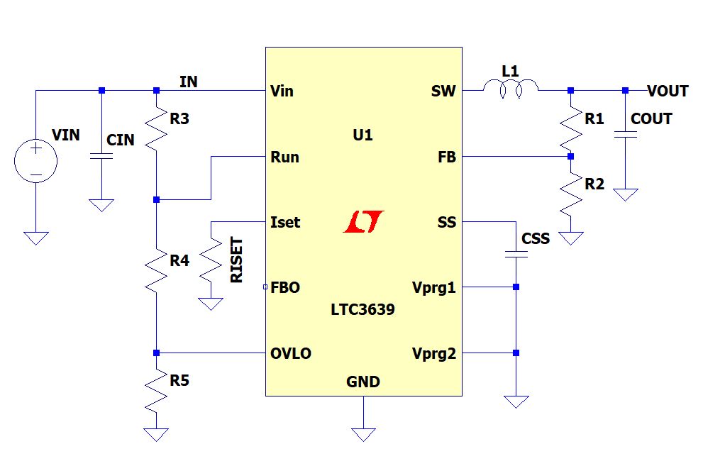
Integrated FET DC-DC Buck Converter Schematic Example
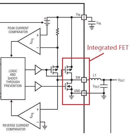
Integrated FET DC-DC Buck Converter Internal Functional Block Diagram
Integrated FET DC-DC Buck Converter PCB Layout Example
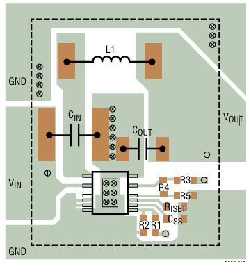
✅ Integrated FET DC-DC Buck Converter PCB Layout Checklist
- SW node isolated and minimal copper area to reduce EMI radiation.
- Input and output capacitors placed as close as possible to IC pins to minimize high-frequency ripple loops.
- Feedback and compensation traces routed away from noisy, high-current switching nodes.
- Use differential or shielded routing on feedback lines longer than 20mm.
- Exposed thermal pads fully soldered with thermal relief patterns and connected to multiple thermal vias.
- Thermal via array implemented under IC with at least 9 vias (0.3mm drill) for effective heat dissipation.
- Maximized copper pour area around IC and inductor for efficient lateral heat spreading.
- Separate analog ground (AGND) and power ground (PGND) planes, connected at a single star ground point close to the IC.
- Gate drive traces kept short, wide, and routed over a solid ground plane to minimize parasitic inductance and ringing.
- No signal traces routed underneath or near the SW node on any PCB layer (top, bottom, or internal).
- Compensation components placed close to the controller IC to minimize loop area and reduce noise susceptibility.
- Use low-ESR ceramic capacitors (X7R) for input and output filtering to ensure stable voltage and reduce high-frequency noise.
- Shielded inductors used and oriented to minimize EMI coupling into sensitive analog or feedback traces.
- All high-current loops minimized in size, especially VIN to CIN to FET to GND loops.
- Avoid 90° bends in high-frequency traces; use smooth or 45° bends to reduce impedance discontinuities.
- Multiple vias used for power and ground connections to reduce resistance and inductance.
- Design review for EMC compliance, including near-field probe measurements of SW node and feedback lines.
- PCB stack-up optimized for controlled impedance and low parasitic capacitance between layers.
- Ensure manufacturing tolerances for solder paste and via plating to maintain reliable thermal and electrical contact.
Conclusion
A robust buck converter layout is a blend of electrical performance, thermal stability, and noise immunity. Whether you’re using external FETs for high power or integrated FETs for compactness, attention to placement, routing, grounding, and thermal design is non-negotiable.
Author Profile
- 20+ years embedded hardware design professional with a burning passion for teaching. Sharing the intricate world of embedded hardware is my mission and joy.
Latest entries
 Tech Updates30 November 2025STM32WBA6: The Next-Generation MCU Powering Secure Short-Range Wireless Designs
 Blogs24 November 2025High-Speed PCB Layout Design Guide-104
 Tech Updates14 September 2025Renesas Launches RL78/L23 Ultra-Low-Power MCUs to Power Smarter Home Appliances
 Blogs7 September 2025High-Speed PCB Layout Design Guide-103