NAND flash memory is a type of non-volatile storage memory (ROM), widely used for data storage in various embedded electronic devices. Its access time, durability, and compact size makes it suitable for applications requiring persistent storage (non-volatile storage).
It’s a type of solid-state memory that stores data by trapping electrons in a floating gate within a transistor. These trapped electrons represent binary information (0s and 1s), allowing data to be stored, and erase electronically.
NAND flash memory is commonly organized into pages and blocks. A page is the smallest unit of data that can be read or written, while a block consists of multiple pages.
When data is written to NAND flash, it’s written at the page level, but erasing can only be done at the block level.
This inherent asymmetry in operations influences wear leveling strategies and the overall management of NAND flash memory to prolong its lifespan.
We will touch upon following topics as a part of this blog:
What are the characteristics and features of NOR Flash Memory?
- Swift Data Access: NAND flash offers fast read and write speeds compared to traditional mechanical storage devices like hard drives. This speed advantage is critical for responsive performance in applications.
- Compact Form Factor: NAND flash memory is incredibly compact, allowing it to be integrated into small devices with limited space, such as smartphones and wearable. NAND flash memories use MLC (Multi-Level Cell) technology, where each cell can store multiple bits of data, increasing storage density. This feature enables high-capacity storage solutions.
- Low Power Consumption: NAND flash memory consumes relatively low power, prolonging battery life in portable devices.
- Structured Page and Block Organization NAND flash is structured into pages (small units for reading and writing data) and blocks (collections of pages). This structure impacts data management strategies.
- Asymmetry in Erase and Write Operations While data can be written at the page level, erasing can only be done at the block level. This characteristic influences wear levelling strategies and management techniques.
- Endurance, Wear Levelling and Lifespan: Different types of NAND flash have varying endurance levels, measured by the number of write/erase cycles they can withstand before becoming unreliable. NAND flash memory employs wear levelling techniques to distribute write/erase cycles across all cells evenly, preventing premature failure of specific cells and extending the memory’s life.
The Architecture of NAND Flash Memory
NAND flash memory cells are connected in a way that resembles a NAND gate. This arrangement involves multiple floating-gate transistors connected in series.
The bit line is pulled low (or read as “1”) only when all the corresponding word lines are pulled high (above the threshold voltage, Vt) for the connected transistors.
This is why NAND flash memory is named as such – it emulates the behaviour of a NAND logic gate “where the output is low only when all inputs are high”.
This configuration allows NAND flash memory to achieve higher density compared to NOR flash, as you can store multiple cells in series along a single bit line, resulting in efficient space utilization.
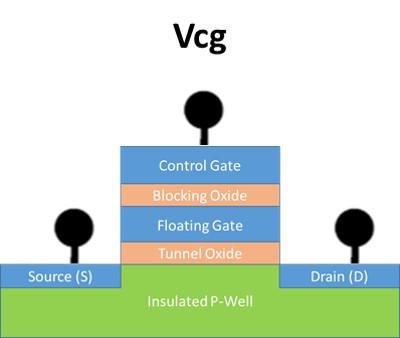 Floating-gate Transistors
 NAND Flash Memory Cell Structure on Silicon
NAND Flash Memory Structure
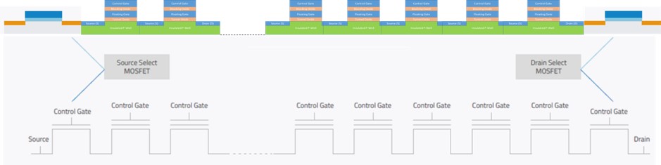
NAND flash memory is organized into blocks. Each block contains a certain number of rows of memory cells. These blocks are the smallest erasable units in NAND flash memory, which means that when data needs to be erased, the entire block must be erased, even if only a portion of it contains valid data.
Within each block, the rows of memory cells are connected together by a common wordline (WL). A wordline is a control line that connects to the control gates of all the memory cells in the same row. When a wordline is activated, it allows for operations like reading, programming, and erasing the cells in that row simultaneously.
The cells along a single word line are logically combined to form a page. In Single-Level Cell (SLC) NAND flash memory, each cell can store one bit of data, so all the cells along a word line contribute to the bits in a page. Below picture shows Layout and wiring details of NAND Flash memory.
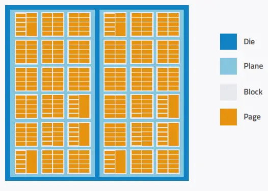
- NAND Page: It is a collection of NAND flash memory cells that are part of the same block and share the same horizontal Control Gate (Word Line). It’s the smallest unit that can be programmed or read within the NAND flash architecture.
- NAND Block: It is composed of multiple NAND Pages. It’s the next higher level of organization within the NAND flash memory structure. Erasing is typically done at the block level, which involves resetting all the pages within the block.
- NAND Plane: Several NAND Blocks are grouped together to form a Plane. A Plane is a higher-level organizational unit that helps manage the programming, reading, and erasing of NAND Blocks.
NAND Flash Memory “Program & Erase”
NAND flash memory arrays are organized into units known as columns or “units.” These units consist of a series connection of transistors in series.
NAND flash memory cells possess two distinct characteristics, A and B as per applied voltage level on of Vth (as shown in below Picture). Characteristic A represents the default state, and characteristic B is the state that’s programmed into the cell.
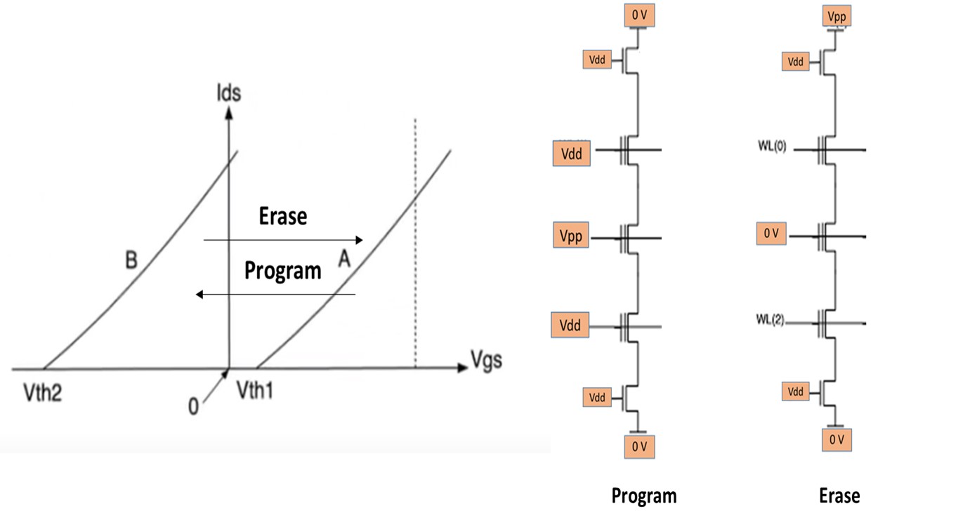
To achieve the short-circuit behaviour required for NAND flash memory, characteristic B is created by turning the transistor into a depletion mode transistor. This type of transistor remains on even when Vgs (gate-source voltage) is zero, acting as a short circuit during reading operations.
Programming NAND Memory
To program a specific cell in NAND flash memory, the goal is to change its characteristics from an “erased” state (logic 1) to a “programmed” state (logic 0). The programming process begins by applying ground (0V) to the Drain terminals on the top and Source terminal on the bottom of the column.
A programming voltage Vpp is applied to the gate of the target cell. Additionally, a positive supply voltage (VDD) to all the intermediate gates of the transistors involved as shown in below picture.
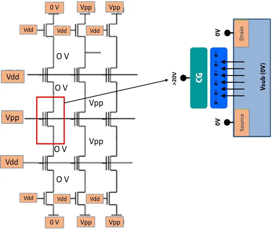 NAND Flash Memory Programming
With the accumulation of electrons on the floating gate, the NAND flash memory cell shifts from acting like a short circuit (ON, characteristic B) to behaving like a transistor in depletion mode (OFF, characteristic A).
This means that the cell becomes non-conductive and can store a logical “0” state. The transformed cell’s non-conductive behaviour allows it to store a logical “0” state (Cell is Programmed). On the other hand programming process does not impact neighbouring cells in the same column.
This is because, other transistors in the Row & column see either 0V on both their drain, source and Vdd on gate terminals or Vpp on both their drain, source and Vdd on gate terminals.
These voltage conditions do not induce tunnelling effects, ensuring that the programming process is localized to the targeted cell.
Erasing NAND Flash Memory
When erasing NAND flash memory cells, a specific set of terminal voltages is applied, creating a large electric field ensuring the flow of electrons from the floating gate into the substrate.
This electron flow back into the substrate causes the formation of an implanted channel, effectively turning the transistor into an effective short circuit (ON).
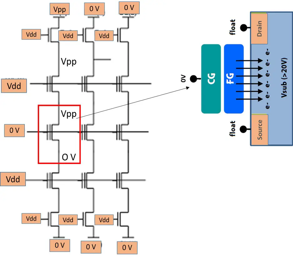
Due to applied voltage configuration as shown in above picture, an electric field is created toward the substrate (negative side).
This electric field facilitates the process of electrons tunneling into the floating gate. As electrons tunnel into the floating gate, the cell transitions from its default characteristic (characteristic B) to characteristic A.
This accumulation of electrons on the floating gate is key to changing the behaviour of the cell. This conditions is call memory cell is programmed.
The challenge during erasing is that all the other transistors in the same column are also exposed to voltages shown in above picture.
As a result, those transistors experience tunnelling effects as well, leading to erase. Unlike NOR flash, where all cells’ values are typically erased, in NAND flash, the impact is more profound because each individual transistor has a unique threshold voltage.
The erasure process can’t be controlled on a per-cell basis, and this variability in threshold voltage makes the situation complex.
To manage this complexity, a strategy is employed where an entire column is reset. First, Programme all cells in the column, ensuring they start from a similar state and have has similar threshold voltage.
Then, the entire column is erased in one operation, effectively clearing the values. The process of writing data into all cells and then erasing them all takes time and involves multiple steps.
This design choice is made to ensure that all cells are roughly aligned in terms of their initial threshold voltage states, which helps ensure a more uniform erasure outcome.
Type of Flash memory
NAND flash memory comes in various types based on their cell configuration and performance characteristics. The main types of NAND flash memory are:
- Single-Level Cell (SLC): SLC NAND flash stores one bit of data per memory cell. This simplicity allows for faster read and write speeds, longer lifespan, and better endurance compared to other types. SLC memory cells have two distinct charge levels, representing logical “0” and “1” states.
- Multi-Level Cell (MLC): MLC NAND flash stores multiple bits of data per memory cell, usually two (2-bit MLC) or sometimes more (3-bit MLC or TLC, 4-bit MLC or QLC). MLC provides higher storage density, making it more cost-effective, but it comes with slower write speeds, lower endurance, and slightly higher error rates compared to SLC.
- 3Triple-Level Cell (TLC): TLC NAND flash stores three bits of data per memory cell. TLC offers even higher storage density but comes with slower write speeds, reduced endurance, and higher error rates compared to MLC.
- 4Quad-Level Cell (QLC): QLC NAND flash stores four bits of data per memory cell. QLC provides the highest storage density among consumer-grade NAND flash types, but it has the slowest write speeds, lowest endurance, and higher error rates.
- 3D NAND: 3D NAND (also known as vertical NAND or V-NAND) stacks memory cells in multiple layers, allowing for increased storage capacity without reducing the chip’s physical size. This technology helps address some of the limitations in write speed, endurance, and storage density present in planar (2D) NAND.
Point to Remember
Definition and Purpose of NAND Flash Memory:
- NAND flash memory is a type of non-volatile storage widely used for data storage in embedded electronic devices.
- It offers high-speed access, durability, and compact size, making it suitable for applications requiring persistent storage.
Cell Configuration and Organization:
- NAND flash memory cells are organized into pages and blocks.
- Pages are the smallest units of data read or written, while blocks contain multiple pages.
- Erasing is done at the block level, influencing wear leveling strategies.
Characteristics and Features:
- NAND flash memory provides fast data access, high storage density, and low power consumption.
- It’s organized into pages and blocks, and operations are asymmetrical (writing at page level, erasing at block level).
- Endurance, wear leveling, and lifespan management are important factors for NAND flash memory’s reliability.
Architecture:
- NAND flash memory cells are connected in series resembling a NAND gate.
- Arrangement involves multiple floating-gate transistors in series, creating efficient space utilization.
Programming NAND Memory:
- Programming involves changing cell characteristics from erased (logic 1) to programmed (logic 0).
- Electric field generated by applied voltage allows electrons to tunnel into the floating gate.
- Accumulated electrons transform cell behavior from short circuit (characteristic B) to depletion mode transistor (characteristic A).
Erasing NAND Flash Memory:
- Erasing involves applying specific terminal voltages to create an electric field that induces electron flow from the floating gate into the substrate.
- This electron flow forms an implanted channel, making the transistor act as a short circuit.
- Neighbouring cells in the same column may also be erased due to voltage exposure.
Management Strategies:
- Writing to all cells and then erasing them all is a strategy to ensure uniform threshold voltage alignment before erasing.
- Ensures that all cells experience similar conditions for erasure.
Types of NAND Flash Memory:
- Types include Single-Level Cell (SLC), Multi-Level Cell (MLC), Triple-Level Cell (TLC), and Quad-Level Cell (QLC).
- Each type offers varying levels of storage density, endurance, and performance characteristics.
- 3D NAND technology allows stacking memory cells in layers for increased capacity.
Author Profile
- 20+ years embedded hardware design professional with a burning passion for teaching. Sharing the intricate world of embedded hardware is my mission and joy.
Latest entries
 Tech Updates30 November 2025STM32WBA6: The Next-Generation MCU Powering Secure Short-Range Wireless Designs
 Blogs24 November 2025High-Speed PCB Layout Design Guide-104
 Tech Updates14 September 2025Renesas Launches RL78/L23 Ultra-Low-Power MCUs to Power Smarter Home Appliances
 Blogs7 September 2025High-Speed PCB Layout Design Guide-103