In our earlier blog High-Speed PCB Layout Design Guide-101, we covered several foundational aspects of high-speed PCB design. These included how to determine whether a design qualifies as high-speed based on factors like knee frequency and trace length, as well as important footprint design considerations to minimize parasitic effects.
We also explored effective floor planning and component placement strategies to ensure optimal signal integrity, discussed best practices for component orientation to support efficient routing and manufacturability, and outlined functional PCB component placement guidelines to balance performance, thermal management, and EMI control.
The subject matter is quite extensive and will therefore be covered across multiple blog posts. This particular blog will focus on the following topics:
What is Transmission Line?
A PCB transmission line is a type of interconnect that carries signals from a transmitter to a receiver on a printed circuit board. It consists of two conductors: a signal trace and a return path—typically a ground plane—with the space between them filled by the PCB’s dielectric material. A key characteristic of signal propagation along a transmission line is its impedance, which exists at every point along the trace. If the trace geometry remains consistent, the impedance stays uniform throughout.
Understanding and accounting for transmission line effects is essential to prevent issues like signal reflections, crosstalk, and electromagnetic interference, all of which can degrade signal quality and lead to errors. A transmission line behaves as a distributed network of resistance (R), inductance (L), and capacitance (C). The two most common types of transmission line structures in PCB design are microstrip and stripline. A third type—coplanar without a reference plane—exists but is rarely used.
|
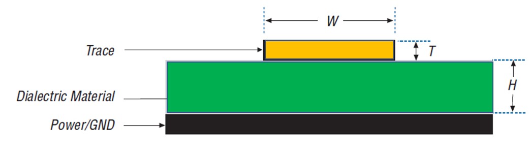
Microstrip Transmission Line Layout
W = width of trace, T = thickness of trace, and H = height between trace and reference plane. |
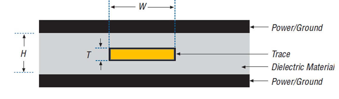
Stripline Transmission Line Layout
W = width of trace, T = thickness of trace, and H = height between trace and reference plane. |
|
Definition A microstrip transmission line consists of a single, uniform signal trace positioned on the outer layer (top or bottom) of a PCB, running parallel to a conducting ground plane that serves as the return path. The signal trace and ground plane are separated by a layer of PCB dielectric material.
|
Definition A stripline consists of a uniform signal trace embedded within the inner layers of a PCB. This trace is sandwiched between two parallel dielectric layers, each followed by a conducting reference plane—providing dual return paths, typically power and/or ground.
|
|
Reference Plane(s) In a microstrip layout, the trace is routed on either the top or bottom layer and is referenced to only one voltage plane—typically a power or ground layer. |
Reference Plane(s) In a stripline layout, the trace is routed on an internal PCB layer and is enclosed between two voltage-reference planes, ensuring symmetrical signal propagation |
|
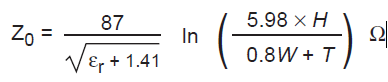
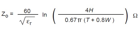
Impedance
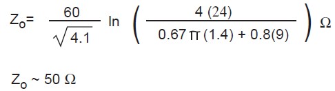
Using typical values of W = 8 mil, H = 5 mil, T = 1.4 mil, and (FR-4) = 4. Microstrip impedance (Zo) yields:
Measurement unit in above Equation is mils (i.e., 1 mil = .001 inches). Also, copper (Cu) trace thickness (T) is usually measured in ounces (i.e., 1 oz = 1.4 mil). |
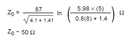
Impedance
Using typical values of W = 9 mil, H = 24 mil, T = 1.4 mil, and (FR-4) = 4.1 Stripline impedance (Zo) yields:
|
|
Impedance Control Easier to design and measure. |
Impedance Control More controlled and stable due to full shielding |
|
Propagation Delay & Mode Faster due to one exposed substrate side. Quasi-TEM mode; dispersion depends on frequency and trace length |
Propagation Delay & Mode Slower due to fully enclosed structure True TEM mode; dispersion-free and frequency-independent. |
|
Electromagnetic Noise More prone to EMI (radiates more) |
Electromagnetic Noise
Better EMI performance (less radiation)
|
| Fabrication Complexity
Simpler, cheaper to manufacture |
Fabrication Complexity
More complex, higher cost |
| Where to Use
· Lower noise environments, simpler stack-ups · Cost-Sensitive and Simple Designs, suitable for many general-purpose, high-speed signals. · Common in RF systems, including antennas, filters, and couplers operating up to several GHz.
|
Where to Use
· Provides superior signal integrity and shielding, making it ideal for critical high-speed or differential pairs in dense multi-layer PCBs. · High-speed, high-density designs with strict signal integrity needs · High Density Interconnect (HDI) boards where space is constrained but performance cannot be compromised. · Suitable for critical Analog or mixed-signal routing. |
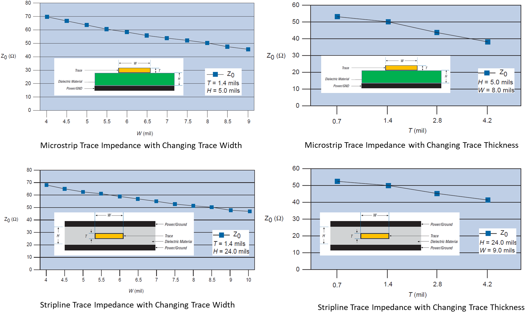
PCB Trace Impedance
Every circuit trace on a PCB has a characteristic impedance, which depends on several factors: the trace width (W), trace thickness (T), the dielectric constant (εr) of the substrate material, and the height (H) between the trace and the reference plane.
Trace Impedance in Microstrip & Stripline
- Impedance in stripline layouts & microstrip layouts, is:
- Inversely proportional to the trace width
- Directly proportional to the distance (height) from the reference planes
- However, in Striplines:
- The rate of impedance change with height is slower than in microstrips
- Structural differences:
- Striplines are fully enclosed in dielectric material (e.g., FR-4)
- Microstrip traces are exposed to air on one side
- Air exposure:
- Lowers the effective dielectric constant in microstrip layouts
- Raises the effective dielectric constant in stripline layouts
- As a result, to achieve the same impedance, stripline designs require greater dielectric thickness. Hence Stripline PCBs with controlled impedance are typically thicker than microstrip PCBs
The image below illustrates how impedance varies in Stripline and Microstrip layouts with changes in trace width and trace thickness. The impedance graphs show that the change in impedance is inversely proportional to trace width and trace thickness.
It provides a clear comparison, demonstrating that the characteristic impedance decreases as the trace width & trace thickness increases.
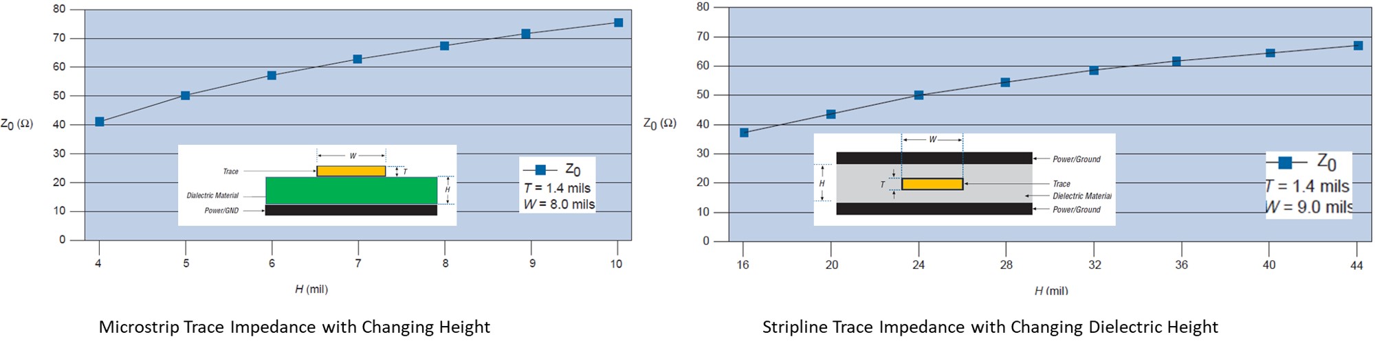
The image below illustrates how impedance varies in Stripline and Microstrip layouts with changes in dielectric height. The impedance graphs show that the change in impedance is directly proportional to trace height above the ground plane.
It provides a clear comparison, demonstrating that the characteristic impedance decreases as the trace thickness increases.
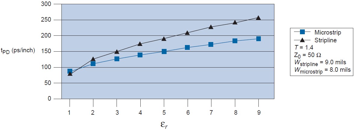
Signal Speed and Propagation Delay Time
A signal cannot pass through a trace with infinite speed. The maximum speed is the speed of light with 3 × 10⁸ m/s. For a certain trace length, the signal needs a certain time to pass it, and this is called the propagation delay time. Propagation delay (tPD) is the time required for a signal to travel from one point to another.
Propagation delay in Stripline: – In Stripline the speed of the signal is a function of the dielectric, which surrounds the trace.
![]()
Propagation delay in Microstrip: – For a microstrip, it is more complicated because the trace is not surrounded by one dielectric. There are at least two: the substrate under the trace and the air above the trace. If the PCB contains a solder mask, a third medium would be present. Here, transmission line propagation delay is a function of the dielectric constant of the material, the trace width, and its distance to the reference plane.
![]()
The figure illustrates the relationship between propagation delay and dielectric constant for both microstrip and stripline traces. As the dielectric constant (εr) increases, the propagation delay (tPD) also increases.
What is Via?
The rise in I/O count has made multi-layer PCBs the industry standard. Signals are routed between different components on the PCB through multiple layers. To enable signal transfer between these layers, vias—plated through-hole conductors—are used. Therefore, having a clear understanding of vias is essential before we proceed further in our discussion.
Vias are holes drilled into a multi-layer PCB that enable electrical connections between different layers. They serve solely to connect layers and do not contain device leads or any reinforcing materials.
Key Parameters Affecting Via Design
1. Via Diameter (Drill and Pad Size)
- Drill Diameter: The size of the hole drilled into the PCB (usually in mm or mils). Smaller drill sizes are needed for HDI and dense layouts.
- Pad Size: The copper ring (annular ring) around the via hole. It ensures a reliable electrical connection and provides mechanical support.
- Why it matters: Determines how much space the via takes on the board and affects manufacturability and reliability.
2. Aspect Ratio (Depth vs. Hole Diameter)
- Definition: The ratio of the PCB thickness (via depth) to the via’s drill diameter.
- Why it matters: A high aspect ratio (e.g., deep and narrow via) is harder to plate uniformly and may cause reliability issues. Lower aspect ratios are preferred for consistent via quality.
3. Plating Thickness
- Definition: The thickness of the copper layer plated inside the via wall during manufacturing.
- Typical Range: 20–25 µm for standard vias, thicker for power vias.
- Why it matters: Ensures good conductivity and mechanical strength. Thicker plating is essential for vias carrying high current or providing thermal conduction.
4. Thermal and Mechanical Reliability
- Definition: The ability of a via to withstand thermal cycling, expansion, and contraction without cracking or delaminating.
- Why it matters: Important in environments with temperature variations. Poorly designed or poorly plated vias can crack, causing open circuits.
5. Signal Integrity (especially at high speeds)
- Definition: The quality of the electrical signal as it travels through the via. Affected by via inductance, capacitance, and impedance discontinuities.
- Why it matters: At high frequencies (e.g., USB 3.0, PCIe, DDR5), vias can introduce reflection, delay, or crosstalk if not properly optimized (e.g., by using via stubs, back-drilling, or controlled impedance design).
Types of Via
The figure below illustrates the different types of vias used in PCB designs. These vias are classified based on their starting and ending layers within the PCB stack-up.
- Through-Hole Via
- Passes through all layers of the PCB (from top to bottom).
- Most common and cost-effective.
- Used for both signal and power connections.
- Blind Via
- Connects an outer layer to one or more inner layers but does not go through the entire board.
- Saves space on densely packed PCBs.
- Buried Via
- Connects only internal layers and is not visible from the outer layers.
- Used in HDI (High-Density Interconnect) boards for compact routing.
Microvias
Microvias are a type of via used in high-density interconnect (HDI) PCBs to connect adjacent layers of a multilayer board. They are significantly smaller in diameter than traditional (through-hole) vias, typically less than 150 µm (or 6 mils), and are often laser-drilled due to their small size.
Key Features of Microvias:
- Size: Hole diameter <150 µm
- Depth: Connects only one or two adjacent layers
- Shape: Typically tapered or conical
- Drilling: Made using laser drilling (not mechanical)
- Filled or Non-filled: May be filled with conductive material, especially if stacked or staggered
High-Speed PCB Design – Key Concepts Summary
📌 1. Transmission Line in PCB
- A transmission line carries signals between transmitter and receiver through a trace and return path (typically ground).
- Two main types:
- Microstrip: Trace on outer layer with ground beneath (asymmetric).
- Stripline: Trace embedded between two ground planes (symmetric).
- Ensuring consistent characteristic impedance is critical for signal integrity.
📌 2. PCB Trace Impedance
- Dependent on: Trace width, thickness, dielectric constant (εr), and height from reference plane.
- Microstrip vs. Stripline:
- Impedance ∝ height, ∝ 1/trace width
- Stripline requires more dielectric thickness for same impedance
- Stripline offers better shielding, but higher cost and complexity
- Impedance is easier to control in stripline, but microstrip is cheaper and easier to fabricate.
📌 3. Signal Speed & Propagation Delay
- Propagation Delay (tPD) is the time a signal takes to travel along a trace.
- Microstrip: Delay affected by air + substrate dielectric.
- Stripline: Delay influenced only by dielectric, offering more predictable performance.
- Higher dielectric constant (εr) = slower signal (more delay).
📌 4. PCB Vias
- Vias are plated holes that connect different PCB layers electrically.
🔹 Types of Vias
- Through-Hole: Connects top to bottom.
- Blind Via: Connects outer to inner layer.
- Buried Via: Connects only inner layers.
- Microvia: Small laser-drilled vias connecting adjacent layers.
🔹 Microvias:
- Used in HDI designs
- Diameter < 150 µm
- Ideal for compact, high-speed PCBs
- May be stacked, staggered, or filled
📌 5. Key Parameters Affecting Via Design
- Via Diameter (Drill & Pad size): Affects space, manufacturability.
- Aspect Ratio: Depth vs. hole diameter—lower is better.
- Plating Thickness: Impacts current capacity and reliability.
- Thermal/Mechanical Reliability: Important for temperature-sensitive applications.
- Signal Integrity: Vias can distort high-speed signals if not optimized
Author Profile
- 20+ years embedded hardware design professional with a burning passion for teaching. Sharing the intricate world of embedded hardware is my mission and joy.
Latest entries
 Tech Updates30 November 2025STM32WBA6: The Next-Generation MCU Powering Secure Short-Range Wireless Designs
 Blogs24 November 2025High-Speed PCB Layout Design Guide-104
 Tech Updates14 September 2025Renesas Launches RL78/L23 Ultra-Low-Power MCUs to Power Smarter Home Appliances
 Blogs7 September 2025High-Speed PCB Layout Design Guide-103