In our previous blog, High-Speed PCB Layout Design Guide-102, we discussed several fundamental concepts essential to high-speed PCB layout design. Key topics included the principles of transmission lines, PCB trace impedance, signal speed and propagation delay, as well as via structures and their impact on performance.
The subject matter is quite extensive and will therefore be covered across multiple blog posts. This particular blog will focus on the following topics.
- PCB Considerations During Circuit Design
- PCB Layer Stack-Up
- PCB Routing
- General Guidelines for Routing Single-Ended
PCB Considerations During Circuit Design
When designing a PCB, several critical factors must be assessed to ensure both performance and reliability. A designer should review the following points before starting the PCB layout design.
- Signal Characteristics: What is the highest operating frequency and the fastest signal rise time in the system?
- Electrical Requirements: Define the electrical specifications at the inputs and outputs of both sources and sinks.
- Sensitive Signals: Identify signals that require special routing considerations—such as controlled impedance, proper termination, or propagation delay (e.g., clocks, buses, and high-speed interfaces).
- Routing Technique: Determine whether a microstrip structure is sufficient for sensitive signals or if a stripline approach is necessary.
- Power Distribution: Assess how many supply voltages are present. Decide whether each requires a dedicated power plane or if plane-splitting is sufficient.
- Functional Block Diagram: Prepare a system diagram showing functional groups (e.g., transmitter path, receiver path, analog, digital, etc.) to organize placement and routing.
- Cross-Group Interconnections: Pay extra attention to signals that interconnect different functional groups. Consider their return paths and potential crosstalk with nearby traces.
- PCB Manufacturer Capabilities: Confirm minimum trace width, spacing, and dielectric thickness with the manufacturer. Check minimum drill size, via requirements, and feasibility of blind or buried vias.
PCB Layer Stack-Up
There are no strict rules on how many layers a PCB should have or what the stack-up must look like; it depends on circuit complexity and performance needs. A simple design with microstrip traces requires at least two layers, with one dedicated to ground, while a four-layer stack (signal–ground–power–signal) is often preferred as it provides better reference planes and power distribution. Planes, in multilayer PCB’s, provide significant reduction in radiated emission over two-layer PCBs. As a rule of thumb, a four-layer board will produce 15 dB less radiation than a two-layer board.
When selecting a multilayer stackup we should consider the following:
- Define the location of each section on the board by means of the functional diagram.
- At which functional block is which supply voltage used?
- It is necessary in high-speed designs to have at least one complete ground plane as a reference for microstrip traces for sensitive signals.
- A signal layer should always be adjacent to a plane. This limits the number of signal
layers embedded between planes to two and top and bottom (outer) layers to one signal.
- Signal layers should be tightly coupled (<10 MIL) to their adjacent planes
- Determine the return path of the signals (which plane will be used). Fast rise time signals take the path of least inductance which is normally the closest plane.
- Cost (the boss’s most important design parameter).
4-Layer PCB Stack-up
Best Practice Recommendation
For a 4-Layer Board
- Use internal ground and power planes (Layer 2 and 3).
- Place signals on outer layers (Layer 1 and 4).
- Ensure signal layers are adjacent to ground for clean return paths.
- Avoid splitting power planes unless absolutely necessary—and use stitching capacitors if you do.
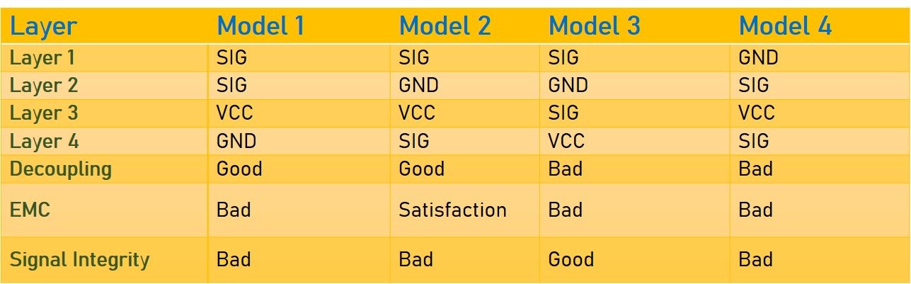
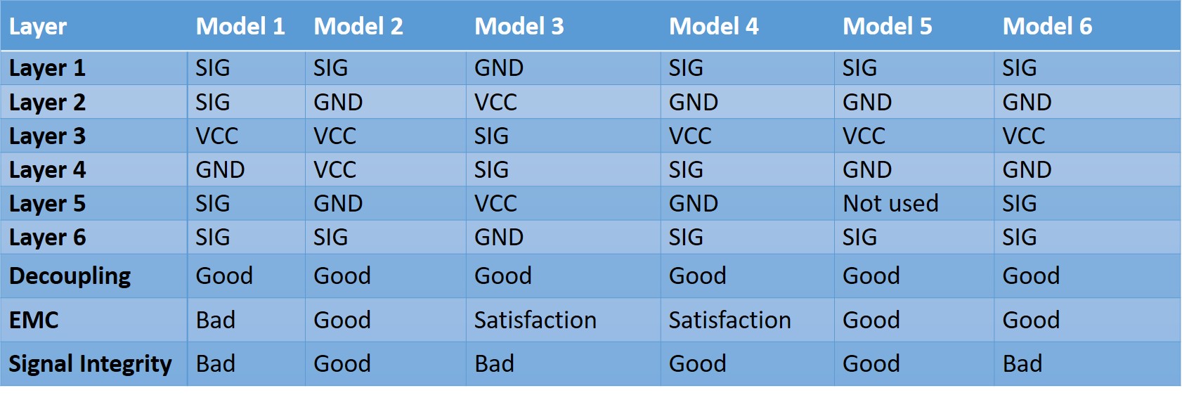
6-Layer PCB Stack-up
Design Tips for 6-Layer PCBs
- Best practice: Place power and ground on internal layers, keeping signals on the outer layers.
- Signal integrity: Ensure every signal layer is adjacent to a solid ground plane for a stable return path.
- EMC: Reduce loop areas and never route signals over split planes.
- Decoupling: Keep VCC and GND planes tightly coupled and support them with adequate bypass capacitors.
- Model comparison: Model 2 is the most robust option for EMC and signal integrity, but it offers only two routing layers. Model 4 provides three signal layers, giving more routing flexibility, but EMC performance is slightly compromised since the ground reference is farther from Layer 4 signals.
PCB Routing
Whether you’re designing a high-speed printed circuit board, good board design practices help ensure your design will work as intended and can be manufactured at volume. In this guide, we’ve compiled some of the essential PCB routing layout guidelines. PCB layout best practices recommend that you always place short, direct traces between components when possible, although this may not always be practical on larger boards.
Printed circuit board design rules and PCB layout guidelines become more complex as the number of layers in your stack-up increases. Such complex designs may need to follow additional board layout guidelines, but the PCB design and layout guidelines shown here are a good place to start for most board designs.
Signal Trace Routing
Proper routing is essential for maintaining signal integrity. To achieve clean trace performance, simulations using reliable Signal Integrity (SI) tools are recommended. There are two primary types of signal traces used in routing:
- Single-ended trace
- Point to Point Routing
- Daisy chain routing
- With stub
- Without stub
- Star routing
- Serpentine routing
- Differential pair trace
General Guidelines For Routing Single-Ended
Point-to-point routing refers to creating a direct electrical connection between two components (a source and a destination) using a single, continuous trace on the PCBng.
- Keep traces short and direct → Minimize length to reduce delay, attenuation, and noise pickup.
- Maintain consistent trace width → Ensures controlled impedance and avoids impedance mismatch, which can cause reflections and SI issues.
- Control trace impedance → Match the trace width, dielectric height, and material properties to achieve the required characteristic impedance (usually 50 Ω).
- Termination: Check whether your single trace requires termination. To prevent overshoot and undershoot, reflections must be minimized. This can be achieved by applying proper termination. Use a suitable termination method (such as series, parallel, Thevenin, or AC termination) to absorb reflections and eliminate signal integrity issues caused by impedance mismatches.
- Minimize via usage → Each via adds parasitic inductance and capacitance; use only if necessary. Do not use vias on traces with sensitive signals, if unnecessary.
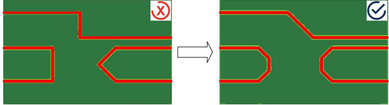
- Avoid sharp corners → Use 45° bends instead of 90° to reduce signal reflection and impedance discontinuities. The best routing would be a round bend specially for the clock and high speed signals.

- Reference a continuous ground plane → High-speed signals should be routed over a solid GND reference plane and not across a plane split or avoid in the reference plane unless absolutely necessary.
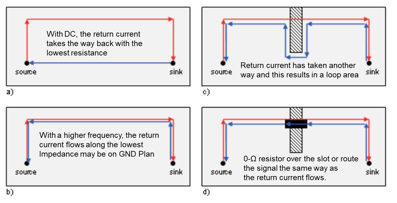
Routing over a split plane
Routing across a plane split or a void in the reference plane forces return high-frequency current to flow around the split or void.
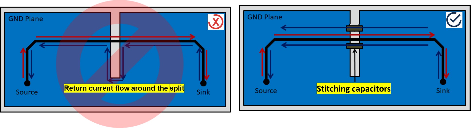
Above figure shows (Left) that the return path must take a longer route than the signal path this can result in the following conditions:
- Excess radiated emissions from an unbalanced current flow
- Delays in signal propagation delays due to increased series inductance
- Interference with adjacent signals
- Degraded signal integrity (that is, more jitter and reduced signal amplitude)
If routing across a plane split cannot be avoided, place stitching capacitors (as shown in the figure on the right) across the split to provide a return path for high-frequency currents. These capacitors help reduce the current loop area and minimize impedance discontinuities caused by crossing the split. Use capacitors of 1 µF or smaller, and position them as close as possible to the plane crossing for maximum effectiveness.
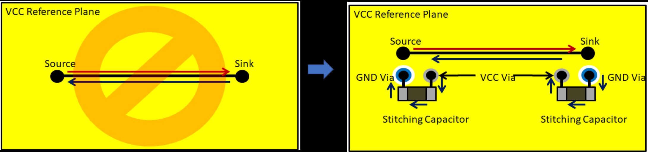
Routing Across Different Reference Planes with AC Capacitor
Avoid altering the reference plane of a high-speed signal trace unless it is absolutely necessary. If crossing between different reference planes cannot be avoided, place AC coupling capacitors to ensure the return current flows alongside the signal path, as shown in the figure on the right.
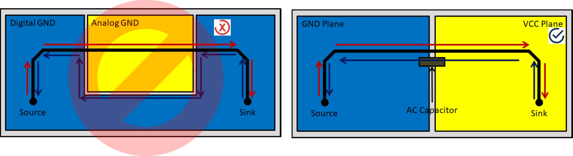
High-Speed Signal References to Power Plane
It is not recommended high-speed signal references to power planes unless it is completely unavoidable. If it is unavoidable it is best to use AC coupling capacitors and ground vias to allow the return signal to have a path back from the sink to the source. Figure 11 depicts the use of AC coupling capacitors and ground vias for the return path.
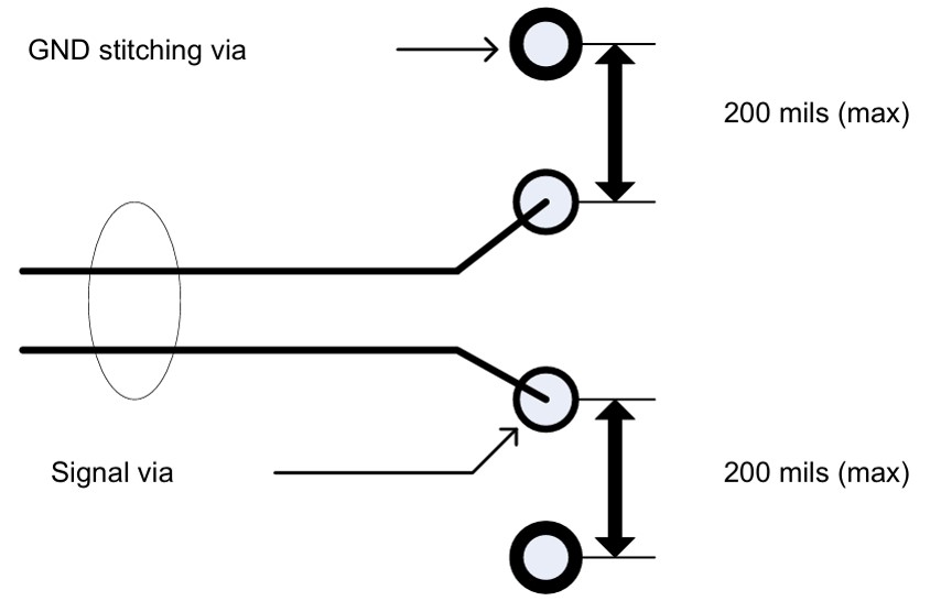
Stitching Reference Vias between Different Grounds
The entirety of any high-speed signal trace should maintain the same GND reference from origination to termination. If unable to maintain the same GND reference, via-stitch both GND planes together to ensure continuous grounding and uniform impedance.
- Spacing from other signals → Follow the guidelines provided in “Routing Strategy to Reduce Crosstalk” section of this blog.
- Avoid routing parallel to high-speed/differential pairs → Prevents unwanted coupling and interference.
- Keep away from noisy areas → Do not route near power supplies, switching regulators, or clock signals.
- Layer changes → If a layer change is necessary, provide proper via stitching to maintain return current continuity.
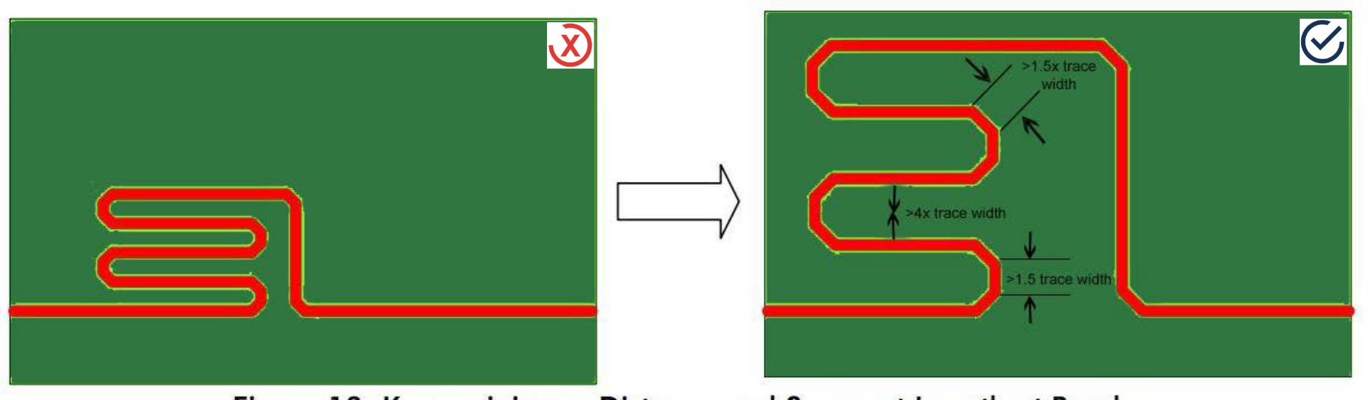
- Length tuning → Only apply if signals require timing alignment; otherwise, keep paths as short as possible. To achieve a required trace length, serpentine routing is often used. When implementing serpentine traces, a minimum spacing of 4 times the trace width should be maintained between adjacent segments of the same trace. Additionally, each bend segment should be at least 5 times the trace width.
- Short Return Path → When a signal travels from a source to a load (e.g., from a microcontroller to a sensor), it doesn’t just disappear—it returns to the source through the lowest resistance return path, typically via the ground plane. With a higher frequency, the return current flows along the lowest Impedance. The loop area is the physical space between the signal trace and its return path.
Return Path Matters because: –
- Reduces EMI (Electromagnetic Interference): A smaller loop area minimizes the antenna effect, reducing radiated emissions.
- Improves Signal Integrity: Shorter return paths reduce inductance and noise, preserving signal shape.
- Prevents Crosstalk: Keeps signals from interfering with adjacent traces.
Best Practices for Shorter Return Paths
- Use continuous ground planes: Avoid splits or gaps that force current to detour.
- Route signal traces close to ground planes: This keeps the return path tight and predictable.
- Add return vias near signal vias: Especially when signals switch layers, to maintain a consistent return path.
- Avoid crossing split planes: This can force the return current to take a longer, noisier route.
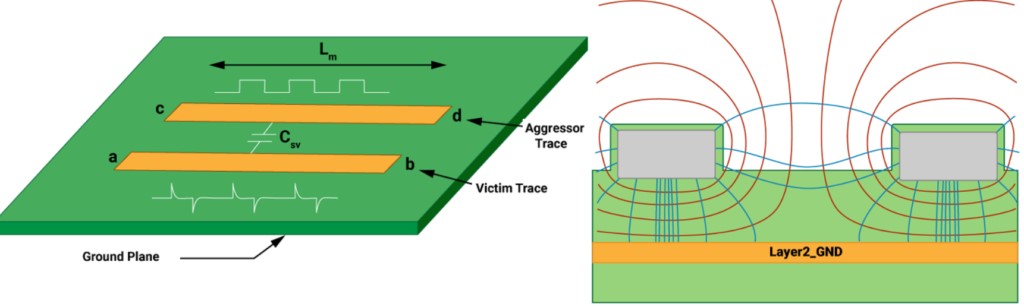
Routing Strategy to Reduce Crosstalk
Crosstalk occurs when a signal in one channel or circuit unintentionally affects another nearby circuit or channel, as illustrated in the image below. This happens due to energy coupling from the “aggressor” signal trace to the “victim” signal trace—usually when two traces are routed close together. Forward crosstalk travels in same direction as the aggressor. It grows with length and increasing aggressor dV/dt, whereas the backward crosstalk travels in the opposite direction as the aggressor and depends only on the aggressor amplitude. Make sure to measure the crosstalk between channels v/s frequency. IEEE802.3KR specifies Insertion Loss Crosstalk Ratio (ICR) which helps quantify how much usable signal remains after accounting for interference. S21 plots show how well signals transmit across frequency, helping validate compliance with IEEE 802.3KR.
Use the following steps to reduce crosstalk in either microstrip or stripline layouts:
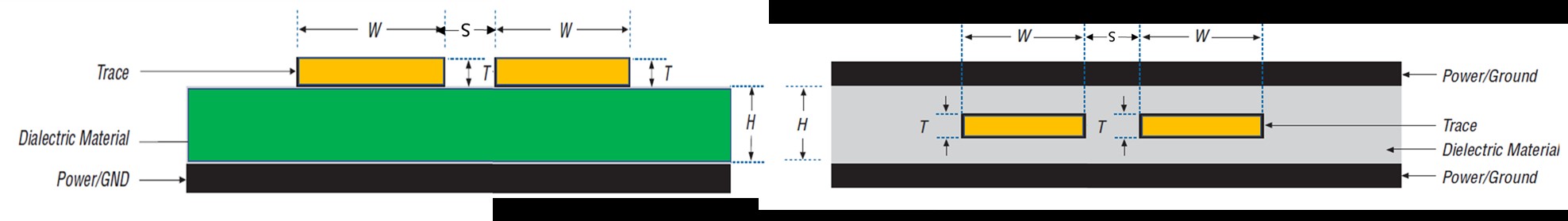
- Increase spacing between signal traces as much as possible; avoid placing them closer than three times the dielectric height(S> 3xH).
- 2W rule:- Keep separation between the line S> 2xW
- Design transmission lines to stay as close as possible to the ground plane, ensuring strong coupling to ground and reducing interaction with nearby signals.
- Use differential routing for critical nets, making sure to match both the trace lengths and the path patterns.
- If strong coupling exists, route single-ended signals on different layers, oriented orthogonally to one another.
- Limit the length of parallel runs for single-ended signals; keep parallel sections short and minimize long coupled paths between nets.
High-Speed PCB Layout Design Guide – Summary
High-Speed PCB Layout Design – Key Guidelines
High-speed PCB design demands careful layer stack planning, controlled impedance routing, continuous ground reference, short return paths, and crosstalk-aware routing. Following these practices ensures better EMC, SI, and overall board performance while staying manufacturable.
1. PCB Considerations During Circuit Design
- Signal characteristics: Identify max frequency and fastest rise time.
- Electrical requirements: Define I/O specs for sources and sinks.
- Sensitive signals: Clocks, buses, and high-speed interfaces need controlled impedance and termination.
- Routing technique: Decide between microstrip or stripline.
- Power distribution: Choose between dedicated power planes or split planes.
- Functional blocks: Group transmitter, receiver, analog, and digital sections.
- Cross-group interconnects: Pay attention to return paths and crosstalk.
- Fabrication limits: Confirm minimum trace width, spacing, dielectric thickness, via types with manufacturer.
2. PCB Layer Stack-Up
- No strict rule—depends on circuit complexity.
- 2-layer: basic designs (signal + ground).
- 4-layer: preferred (signal–ground–power–signal) → reduces EMI by ~15 dB vs 2-layer.
- Key practices:
- Always include at least one full ground plane.
- Place signal layers adjacent to planes (<10 mil spacing).
- Return current follows the lowest inductance path (nearest plane).
- Use stitching capacitors or vias when crossing splits to provide a high-frequency return path.
3. Signal Trace Routing
- General rules for single-ended routing:
- Keep traces short, direct, and consistent in width.
- Control impedance (typically 50Ω).
- Apply proper termination (series, parallel, Thevenin, or AC).
- Minimize via use.
- Use 45° or curved bends, avoid 90°.
- Always reference a continuous ground plane.
- Avoid routing across plane splits—use stitching capacitors if unavoidable.
- Trace types:
- Single-ended: point-to-point, daisy-chain (with/without stub), star, serpentine.
- Differential pair: for high-speed interfaces, matched length and path.
4. Return Path & Shorter Loops
- Why it matters: Smaller loop areas reduce EMI, improve SI, and prevent crosstalk.
- Best practices:
- Use continuous ground planes.
- Route signals close to ground.
- Place return vias near signal vias.
- Avoid split planes.
5. Crosstalk Reduction
- Caused by coupling between nearby traces (forward/backward crosstalk).
- Guidelines:
- Maintain spacing: S > 3× dielectric height (or ≥ 2× trace width).
- Keep traces close to ground planes.
- Use differential routing for critical nets.
- Route signals orthogonally on adjacent layers.
- Minimize long parallel runs.
- Validate with crosstalk measurements (ICR, S21 plots).
Author Profile
- 20+ years embedded hardware design professional with a burning passion for teaching. Sharing the intricate world of embedded hardware is my mission and joy.
Latest entries
 Tech Updates30 November 2025STM32WBA6: The Next-Generation MCU Powering Secure Short-Range Wireless Designs
 Blogs24 November 2025High-Speed PCB Layout Design Guide-104
 Tech Updates14 September 2025Renesas Launches RL78/L23 Ultra-Low-Power MCUs to Power Smarter Home Appliances
 Blogs7 September 2025High-Speed PCB Layout Design Guide-103