In our earlier blog post, High-Speed PCB Layout Design Guide-103, we explored essential routing strategies such as thoughtful layer stack configuration, controlled impedance paths, maintaining a consistent ground reference, minimizing return path lengths, and mitigating crosstalk. Adhering to these principles not only enhances electromagnetic compatibility (EMC) and signal integrity (SI), but also contributes to a high-performance, manufacturable PCB design.
As the subject matter is quite extensive and will therefore be covered across multiple blog posts. This particular blog will focus on the following topics: –
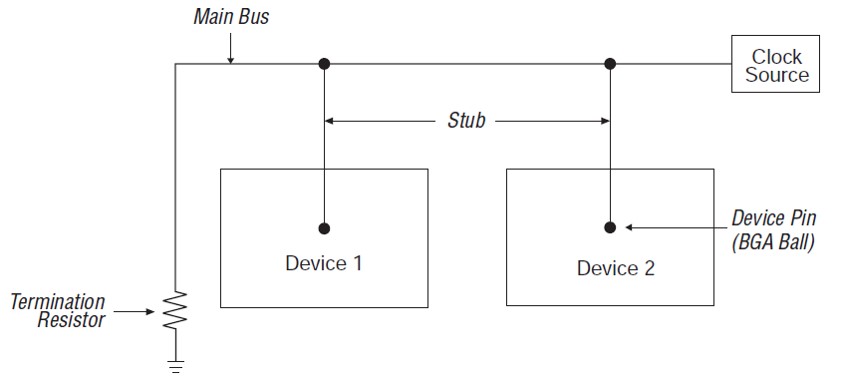
Daisy Chain Routing with Stubs
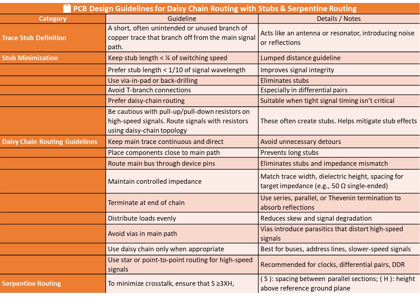
Daisy chain routing is a PCB routing technique where multiple components (loads) are connected sequentially along a single trace path, where Devices are connected in series along the main trace. A stub refers to an undesirable portion of a trace or via that can negatively affect signal integrity, especially in high-speed circuits. To maintain consistent impedance and minimize reflections, stub lengths should be kept as short as possible. While it may not always be feasible to eliminate stubs entirely, careful routing practices are essential to manage their impact effectively.
Via Stub
When a via connects only partway through a multilayer PCB, the leftover portion is called a stub. It doesn’t carry signal but can reflect it, causing distortion.
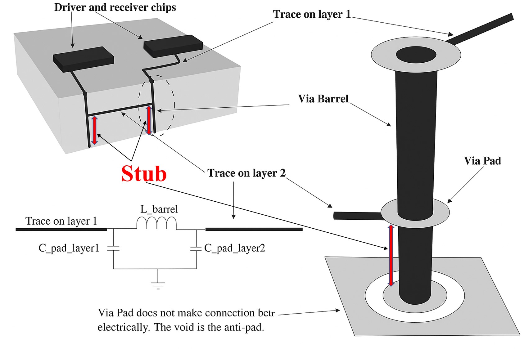
Trace Stub
A PCB trace stub is a short, often unintended or unused branch of copper trace that splits off from the main signal path. While sometimes unavoidable, it can disrupt signal integrity—particularly in high-speed digital circuits—by introducing reflections and impedance mismatches.
Why Are Trace Stubs a Problem?
- Signal Reflection: Stubs act like open-ended transmission lines, reflecting signals back toward the source. This can interfere with the original signal.
- Impedance Discontinuity: They introduce mismatches in impedance, which degrade signal quality.
- Increased Crosstalk and EMI: Stubs can radiate electromagnetic interference and pick up noise from nearby traces.
- Timing Errors: In high-speed circuits, even small stubs can introduce deterministic jitter and bit errors, especially in differential pairs or clock lines
Design Tips to Prevent Signal Reflections from Stubs
- Keep stub lengths shorter than one-quarter of the driver’s switching speed (lumped distance) to minimize reflections.
- For optimal signal integrity, aim for stub lengths less than one-tenth of the signal’s wavelength.
- Maintain disciplined routing practices to avoid unnecessary branches and ensure direct signal paths.
- Utilize simulation tools to analyze and address signal integrity issues related to stubs.
- Consider back-drilling to remove unused via stubs in multilayer boards—though effective, this method is costly and typically reserved for ultra-high-speed designs where absolutely necessary.
- Use via-in-pad where Places vias directly under component pads to reduce stub length. Blow pictures show how Via on Pad reduces the Stub length compare to Traditional Via.
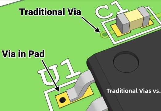
Via-in-Pad (VIP) technology is widely adopted across industries that demand high performance and compact design, such as mobile devices, aerospace and defence systems, medical equipment, and automotive electronics.
Despite its manufacturing complexity and higher cost, VIP offers compelling advantages—including greater routing density, enhanced signal integrity, and superior thermal management—making it a valuable solution for advanced electronic designs.
- Avoid T-branch connections, especially in differential pairs. We will discuss more on this in coming blogs.
- Prefer daisy-chain routing over T-branches when tight signal timing isn’t critical.
- Be cautious with pull-up or pull-down resistors on high-speed signals, as they often create stubs.
- If such resistors are necessary, route the signals using a daisy-chain topology.
Daisy-chain topology
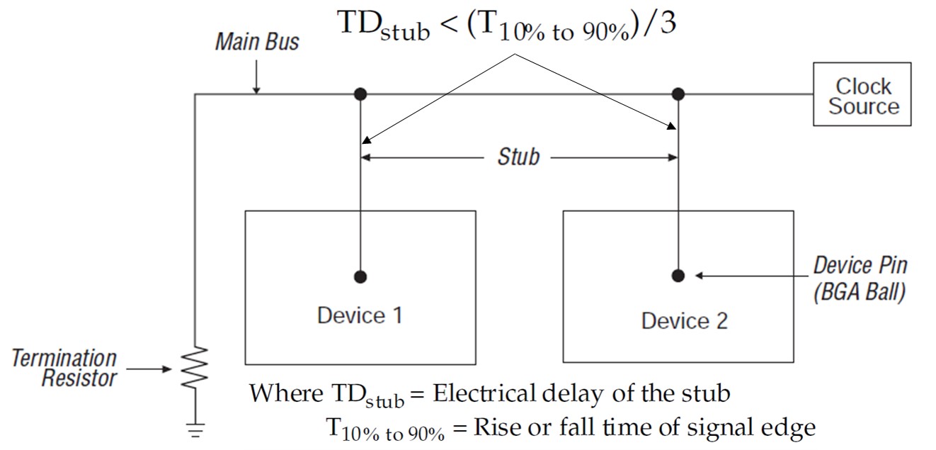
Daisy chain routing is a widely used technique in PCB design. However, one drawback is the need for stubs as explained above. If these stubs are excessively long, they can cause transmission line reflections, leading to degraded signal integrity. To mitigate this, stub lengths must be kept within specific limits, as outlined below
Daisy Chain Routing Guidelines
Here are some layout guidelines for Daisy Chain Routing in PCB design:
- Keep the main trace continuous and direct
- Route the primary signal path without unnecessary detours to minimize reflections and delay.
- Place components close to the main path
- Keep devices aligned along the chain to avoid long stubs.
- Minimize stub length
- Stub lengths must be kept within specific limits as explained below.
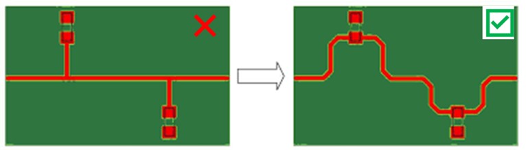
- Daisy Chain Routing without Stub
- Try daisy chain routing with the main bus running through the device pins, eliminating stubs.
- This layout removes the risk of impedance mismatch between the main bus and the stubs, minimizing signal integrity problems.
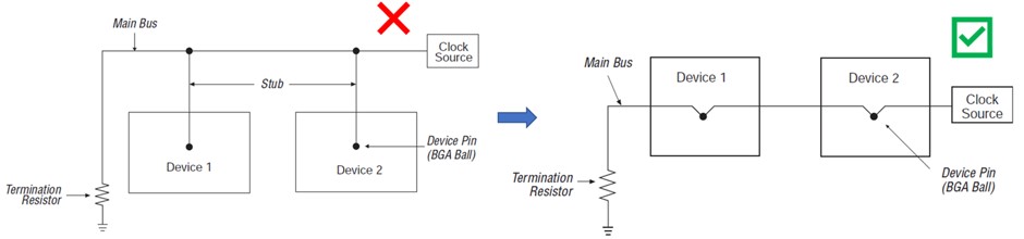
Daisy Chain Routing without Stub
- Maintain controlled impedance & Terminate at the end of the chain
- Match the trace width, dielectric height, and spacing to achieve the target characteristic impedance (e.g., 50 Ω single-ended).
- Apply proper termination (series, parallel, or Thevenin) at the final load to absorb reflections. Few of the examples are as shown below.
- Distribute loads evenly along the chain if possible to reduce skew and signal degradation.
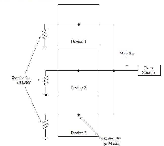
Star Routing with Termination Schema
In star routing, the clock signal is distributed simultaneously to all connected devices (as illustrated in the figure below). To minimize clock skew, it’s essential to match the trace lengths between the clock source and each device. Additionally, maintaining identical load characteristics across all branches helps preserve signal integrity. For optimal performance, the impedance of the main bus should be matched with that of the long traces connecting to the individual devices. A proper termination scheme must be implemented to ensure impedance matching throughout the entire clock path—from the source to each individual device. This prevents impedance mismatches and helps mitigate signal integrity issues.
- Avoid vias in the main path
- Use vias only if absolutely necessary, as they introduce parasitics that can distort high-speed signals.
- Use daisy chain only when appropriate
- This routing method is best for buses, address lines, or slower-speed signals. For high-speed signals like clocks, differential pairs, or DDR, star routing or point-to-point may be more reliable.
Serpentine Routing
When a design requires equal-length traces between the source and multiple loads, you can bend some traces to match trace lengths (see Figure below). Improper trace bending affects signal integrity and propagation delay.
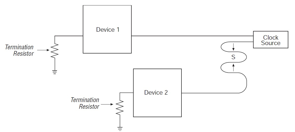
To minimize crosstalk, ensure that S ≥3XH, where S is the spacing between the parallel sections and H is the height of the signal trace above the reference ground plane.
Design Guidelines for Daisy Chain Routing with Stubs & Serpentine Routing – Summary
Author Profile
- 20+ years embedded hardware design professional with a burning passion for teaching. Sharing the intricate world of embedded hardware is my mission and joy.
Latest entries
 Tech Updates30 November 2025STM32WBA6: The Next-Generation MCU Powering Secure Short-Range Wireless Designs
 Blogs24 November 2025High-Speed PCB Layout Design Guide-104
 Tech Updates14 September 2025Renesas Launches RL78/L23 Ultra-Low-Power MCUs to Power Smarter Home Appliances
 Blogs7 September 2025High-Speed PCB Layout Design Guide-103