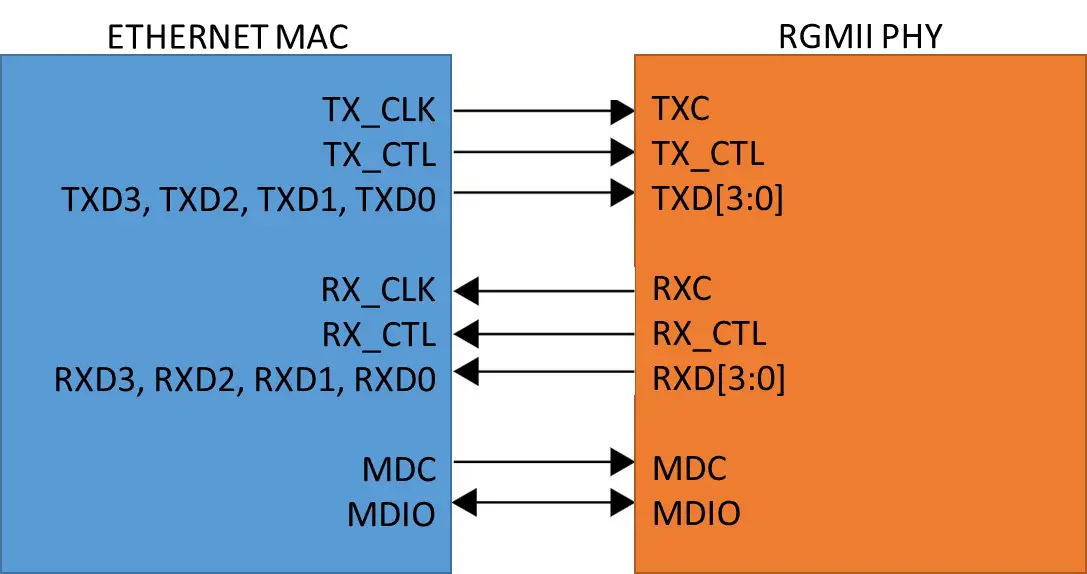
RGMII stands for Reduced Gigabit Media Independent Interface. It is a standard used to connect Ethernet PHYs (Physical Layer devices) to MACs (Media Access Controllers). The RGMIl is intended to be an alternative to the IEEE802.3u MIl, the IEEE802.32 GMil. The principle objective is to reduce the number of pins required to interconnect the MAC and the PHY from 24 pins for GMII to 12 pins for RGMII interface. In order to accomplish this objective, the data paths and all associated control signals are reduced and are multiplexed.
RGMII is the most common interface because it supports 10 Mbps, 100 Mbps, and 1000 Mbps connection speeds at the PHY layer. RGMII uses four-bit wide transmit and receive data paths, each with its own source-synchronous clock. All transmit data and control signals are source synchronous to TX_CLK, and all receive data and control signals are source synchronous to RX_CLK.
For all speed modes, TX_CLK is sourced by the MAC, and RX_CLK is sourced by the PHY. In 1000 Mbps mode, TX_CLK and RX_CLK are 125 MHz, and Dual Data Rate (DDR) signaling is used. In 10 Mbps and 100 Mbps modes, TX_CLK and RX_CLK are 2.5 MHz and 25 MHz, respectively, and rising edge Single Data Rate (SDR) signaling is used.
RGMII (Reduced Gigabit Media Independent) Interface Block Diagram
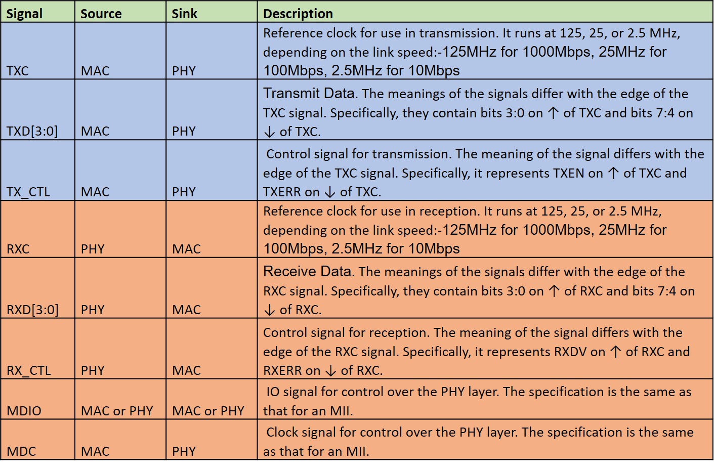
The Reduced Gigabit Media Independent Interface (RGMII) supports speeds up to 1 Gbps with a clock rate of 125 MHz. Signal descriptions are provided in Table below.
RGMII operation
All RGMII signals are positive logic. The 8-bit data is multiplexed by taking advantage of both clock edges (↑ of TXC /RXC and bits ↓ of TXC/RXC). The lower 4 bits are latched on the positive clock edge and the upper 4 bits are latched on trailing clock edge. The control signals are multiplexed into a single clock cycle using the same technique
- The MAC sources the transmit reference clock, TXC, at 125MHz for 1000Mbps, 25MHz for 100Mbps, and 2.5MHz for 10Mbps.
- The PHY recovers and sources the receive reference clock, RXC, at 125MHz for 1000Mbps, 25MHz for 100Mbps, and 2.5MHz for 10Mbps.
- For 1000Base-T, the transmit data, TXD [3:0], is presented on both edges of TXC, and the received data, RXD [3:0], is clocked out on both edges of the recovered 125MHz clock, RXC.
- For 10Base-T/100Base-TX, the MAC holds TX_CTL low until both PHY and MAC operate at the same speed. During the speed transition, the receive clock is stretched on either a positive or negative pulse to ensure that no clock glitch is presented to the MAC.
- TX_ER and RX_ER are combined with TX_EN and RX_DV, respectively, to form TX_CTL and RX_CTL. These two RGMII control signals are valid at the falling clock edge.
Several RGMII PHY has the option to source a 125MHz reference clock on the CLK125_NDO pin. This clock provides a lower-cost reference clock alternative for RGMII MACs that require a 125MHz crystal or oscillator.
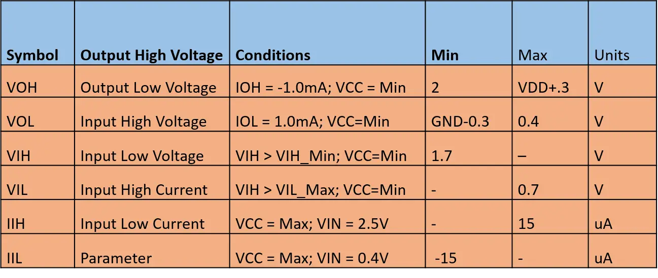
Electrical Characteristics
The RGMII (including MDIO/MDC) will be based upon 2.5V CMOS interface voltages as defined by JEDEC EIA/JESD8-5.
- In version 1.3, all signals including MDIO and MDC are defined as operating with 2.5-V CMOS interface voltages. As per JEDEC EIA/JESD8-5.
- In version 2.0, on the other hand, they are defined as operating with 1.5-V HSTL interface voltages. As per JEDEC EIA/JESD8-6.
RGMII Timing Specification
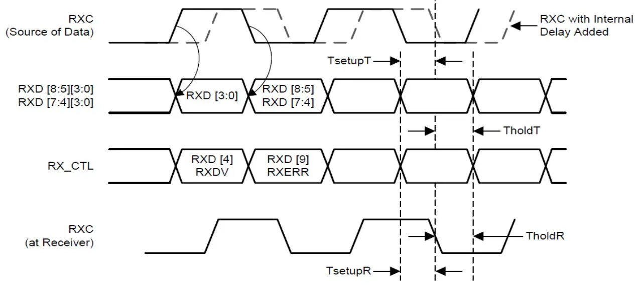
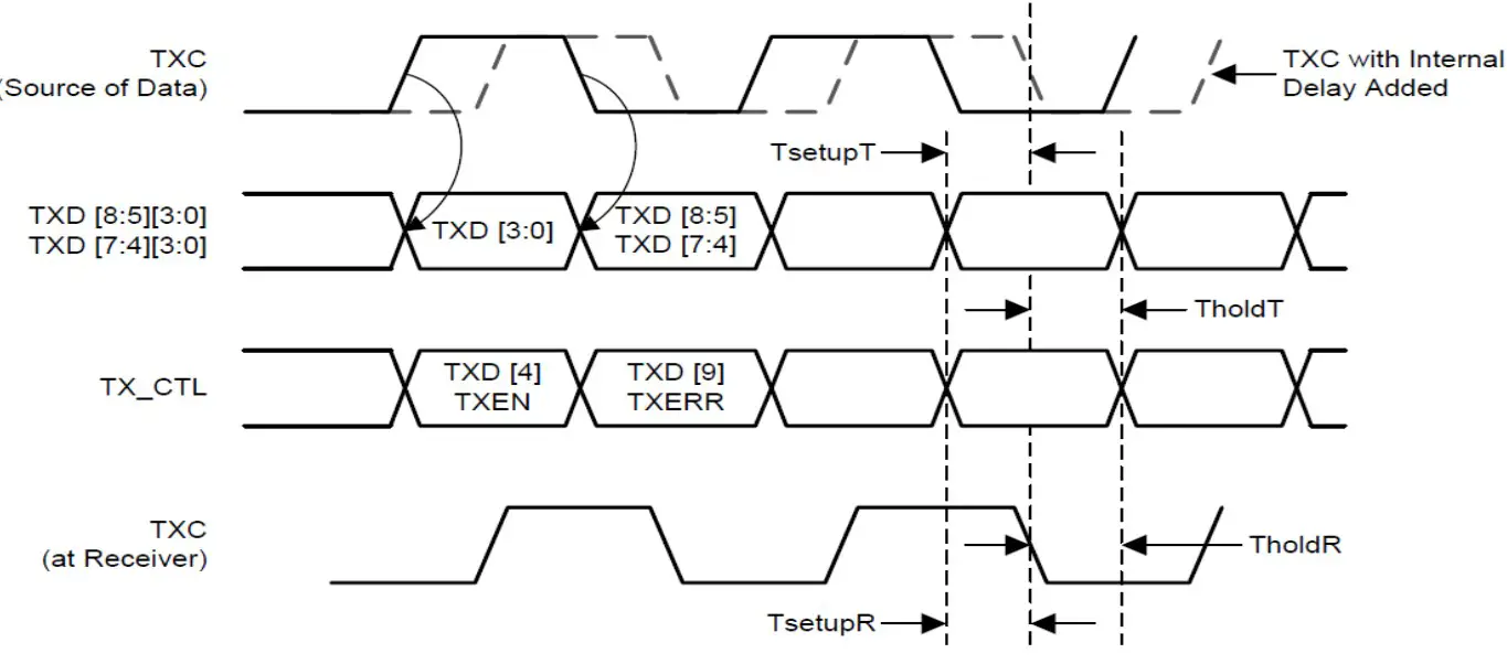
RGMII specifies that the clock and data will be generated simultaneously by the transmitting source which requires a skew be introduced between clock and data. The skew can be achieved by PCB trace routing or by an internal delay in the transmitting or receiving node. The skew imposed on the clock and data shall be chosen carefully to ensure meeting the requirements of the interface as described in the next section.
The RGMII defines two types of timing specification as the original RGMII and the RGMII-ID. While the timing specification in the version 1.3 and earlier is called the original RGMII, the timing specification in version 2.0 is called RGMII-ID.
The difference between the original RGMII and the RGMII-ID is following:
- Original RGMII(V1.3): – Clock signals must be delayed from 1.5 ns to 2.0 ns relative to the data signals. This delay is implemented by PCB design.
- RGMII-ID(V2.0): – Clock signals must be delayed at least 1.2 ns relative to the data signals. This delay is implemented by the internal design of the MAC devices.
RGMII RX Timing Diagram
RGMII TX Timing Diagram
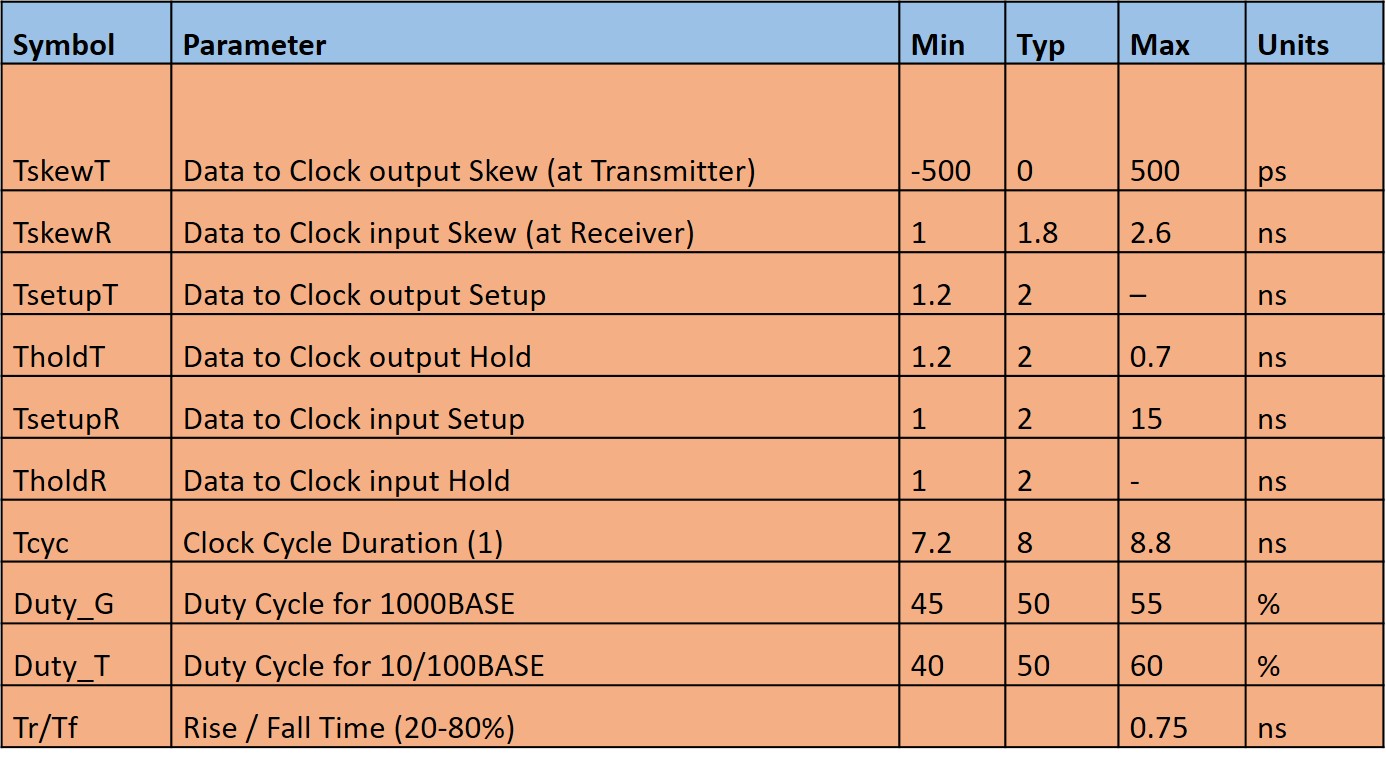
RGMII v2.0 Timing Requirements
Auto-Negotiation
RGMII PHY conforms to the auto-negotiation protocol, defined in Clause 28 of the IEEE 802.3 Specification. Auto-negotiation allows UTP (unshielded twisted pair) link partners to select the highest common mode-of-operation. During auto-negotiation, link partners advertise capabilities across the UTP link to each other, and then compare their own capabilities with those they received from their link partners. The highest speed and duplex setting that is common to the two link partners is selected as the operating mode.
The following list shows the speed and duplex operation mode from highest-to-lowest.
- Priority 1: 1000Base-T, full-duplex
- Priority 2: 1000Base-T, half-duplex
- Priority 3: 100Base-TX, full-duplex
- Priority 4: 100Base-TX, half-duplex
- Priority 5: 10Base-T, full-duplex
- Priority 6: 10Base-T, half-duplex
If auto-negotiation is not supported or the PHY link partner is forced to bypass auto-negotiation for 10Base-T and 100Base-TX modes, the PHY sets its operating mode by observing the input signal at its receiver. This is known as parallel detection, and allows the RGMII PHY to establish a link by listening for a fixed signal protocol in the absence of the auto-negotiation advertisement protocol.
Summary
RGMII (Reduced Gigabit Media Independent Interface) is a standard designed to connect Ethernet PHYs (Physical Layer devices) to MACs (Media Access Controllers). It is intended as an alternative to IEEE802.3u MII and IEEE802.3z GMII. The primary objective is to reduce the number of pins required for interconnection from 24 pins in GMII to 12 pins in RGMII by reducing and multiplexing data paths and control signals.
Key Features
- Pin Reduction: RGMII reduces the pin count from 24 (in GMII) to 12 by using both rising and falling clock edges for data transfer.
- Speed Support: Supports 10 Mbps, 100 Mbps, and 1000 Mbps (1 Gbps) speeds.
- Data Paths: Uses 4-bit wide transmit (TXD) and receive (RXD) data paths with source-synchronous clocks (TXC and RXC).
- Clock Signals: TXC is sourced by the MAC and RXC by the PHY, with frequencies of 125 MHz (1000 Mbps), 25 MHz (100 Mbps), and 2.5 MHz (10 Mbps).
- Signaling: Utilizes DDR (Double Data Rate) signaling at 1000 Mbps and SDR (Single Data Rate) signaling at lower speeds.
Signal Descriptions
- TXC (MAC to PHY): Transmission reference clock, varies with speed.
- TXD[3:0] (MAC to PHY): Transmit data, with data bits multiplexed on clock edges.
- TX_CTL (MAC to PHY): Transmit control signal, multiplexed as TXEN and TXERR.
- RXC (PHY to MAC): Reception reference clock, varies with speed.
- RXD[3:0] (PHY to MAC): Receive data, with data bits multiplexed on clock edges.
- RX_CTL (PHY to MAC): Receive control signal, multiplexed as RXDV and RXERR.
- MDIO (MAC or PHY): Bi-directional signal for control over the PHY layer.
- MDC (MAC to PHY): Clock signal for MDIO.
RGMII Operation
- Data Multiplexing: 8-bit data is multiplexed using both clock edges, with lower 4 bits latched on the rising edge and upper 4 bits on the falling edge.
- Control Signals: TX_ER and RX_ER are combined with TX_EN and RX_DV to form TX_CTL and RX_CTL.
- Clock and Data Skew: Requires skew between clock and data for proper timing, which can be implemented via PCB trace routing or internally in devices.
Electrical Characteristics
- Voltage Levels: Operates with 2.5V CMOS interface voltages (version 1.3) and 1.5V HSTL interface voltages (version 2.0).
- Input/Output Characteristics: Defines voltage thresholds and current levels for proper signal integrity.
Timing Specifications
- Original RGMII (v1.3): Clock signals must be delayed by 1.5 to 2.0 ns relative to data signals, typically via PCB design.
- RGMII-ID (v2.0): Clock signals must be delayed by at least 1.2 ns relative to data signals, implemented internally by MAC devices.
- Timing Requirements: Specifies data to clock skew, setup and hold times, clock cycle duration, and rise/fall times.
Auto-Negotiation
- Protocol: Conforms to IEEE 802.3 Clause 28 auto-negotiation protocol, allowing devices to select the highest common mode of operation.
- Priority: Establishes speed and duplex mode priorities from highest (1000Base-T full-duplex) to lowest (10Base-T half-duplex).
- Parallel Detection: If auto-negotiation is bypassed, PHY establishes a link by detecting fixed signal protocols.
Author Profile
- 20+ years embedded hardware design professional with a burning passion for teaching. Sharing the intricate world of embedded hardware is my mission and joy.
Latest entries
 Tech Updates30 November 2025STM32WBA6: The Next-Generation MCU Powering Secure Short-Range Wireless Designs
 Blogs24 November 2025High-Speed PCB Layout Design Guide-104
 Tech Updates14 September 2025Renesas Launches RL78/L23 Ultra-Low-Power MCUs to Power Smarter Home Appliances
 Blogs7 September 2025High-Speed PCB Layout Design Guide-103