In today’s world, the complexity of electronic products has grown significantly due to increasing demands for higher performance—such as faster data transfer rates, advanced image processing, greater computing power, and expanded functionality.
As a result, modern PCBs are now designed with higher component densities and operate at signal frequencies exceeding 5 GHz. They also integrate a wide range of high-speed interfaces, including, DDR4/5/6/7, PCIe 4.0/5.0/6.0, USB 3.0, Gigabit Ethernet, and advanced display standards like HDMI2.1b (8K, Videos, 48Gbps) MIPI, DSI, and LVDS, among others. These demands are also driving the development of advanced PCB technologies, such as High Density Interconnect (HDI), which utilize blind and buried microvias to support increased complexity and performance requirements.
Looking ahead, the push for even greater performance in computers, mobile devices, and communication systems will require PCB designs capable of handling even faster speeds and more densely packed components. This blog explores the key challenges of high-speed PCB design and outlines best practices to effectively address them.
The subject matter is quite extensive and will therefore be covered across multiple blog posts. This particular blog will focus on the following topics: –
- How to Decide if your design is a High-Speed Design
- Footprint Design Considerations
- Floor Planning & Component Placement Strategies
- Component Orientation and Placement Strategies
- Functional PCB Component Placement Guidelines
How to Decide if your design is a High-Speed Design
There’s no absolute frequency threshold beyond which a signal is universally considered “high-speed,” but as a general guideline, if the knee frequency (Fk), which is a factor of rise time exceeds 100 MHz and PCB trace lengths extend beyond a few inches, transmission line effects such as reflections, crosstalk, and impedance mismatches become significant and must be addressed in the design.
Knee Frequency & Rise time
To begin with, system designers must specify one or more of the following parameters, which define the high-speed characteristics of the circuitry:
- The knee frequency (Fk), is a crude estimate of the highest frequency content in the highest-speed signals within the circuit
- The fastest rise or fall time (Tr) of the digital signals
- The maximum data transfer rate (DTR) relevant to the circuit’s signals
Fk ≈ 0.5 / F10.90% ≈ 2.5 DTR
Let’s take an example of rise times ≤ 5 ns, the knee frequency exceeds 100 MHz
A signal is considered high-speed when its knee frequency is:
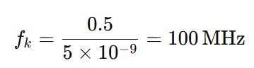
- As a rough rule of thumb knee frequency (Fk), > 100 MHz — this is where transmission line effects (like reflections, crosstalk, and impedance mismatches) become significant on typical PCB traces.
- So, if Tr ≤ 5 ns, treat the signal as high-speed for PCB design purposes.
Knee Frequency & Trace Length
A signal is considered high-speed when the knee frequency approaches or exceeds the point where, PCB trace length becomes a significant fraction of the signal wavelength
General Rule of Thumb:
A signal is high-speed when: 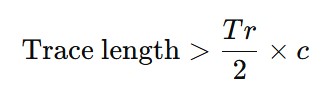
Where:
- Tr = signal rise time
- c = speed of signal propagation on the PCB (~6 inches/ns or ~15 cm/ns for FR-4)
Let’s take an example of rise times of 1 ns:
- Knee frequency = 0.5 / 1 ns = 500 MHz
- If trace length > 3 inches (~7.5 cm), treat the signal as high-speed
This means:
- If the interconnect length l < 9.8 inches (as in most PCBs smaller than 8″ x 8″), the signal can be treated as low-speed.
- If l ≥ 9.8 inches (which may occur even on a 6″ x 8″ board depending on routing), the signal must be treated as high-speed.
Knee Frequency, Interconnect length & Wavelength
While the above rule of thumb works well in most scenarios, there are special cases where even signals with a knee frequency as low as 60 MHz may require high-speed design considerations.
Wavelength of the signal at Knee frequency (Fk): λm = v / Fk
Where:
v = speed of signals on a PCB ≈ 6.9 in/ns (microstrip) and 5.9 in/ns (stripline).
λₘ = signal wavelength in the PCB material
Propagation Delay on PCB: tpd = 1/ v
Now a rule of thumb considering interconnect length:
- If interconnect length l < λₘ /12, high-speed effects can be ignored.
- If interconnect length l ≥ λₘ /12, treat it as a high-speed interconnect and apply transmission line design practices.
Let’s take an example of signal with Fk = 60 MHz
- For a signal with Fk = 60 MHz,
- Minimum wavelength in PCB material (λₘ) is:
λₘ = 5.9 in/ns ÷ 60 MHz = 98.3 inches
Then, λₘ /12 = 98.3 / 12 ≈ 8.2 inches
Thus, if the interconnect length l < 8.2 inches, it can be treated as low-speed. However, if l ≥ 8.2 inches, it should be considered a high-speed interconnect.
Hence, it’s essential to evaluate knee frequency, rise time, interconnect length, and signal wavelength to determine if your design qualifies as high-speed. Analyze which of the above criteria best applies to your design, perform the necessary calculations, and, if high-speed behavior is indicated, implement appropriate design practices to ensure signal integrity and reliable performance.
High-Speed PCB Layout Design
Now that we understand our design meets the criteria for high-speed operation, it’s crucial to approach it with appropriate care. High-speed PCB layout demands meticulous attention to several key aspects, including footprint design, PCB floor planning, component placement, layer stack-up, and trace routing. This blog explores the essential layout design requirements necessary to ensure reliable performance in high-speed designs.
High-Speed PCB: – Footprint Design Considerations
In high-speed PCB design, careful attention must be given to footprint pad sizes, as they directly impact signal integrity and manufacturing reliability. While standard pad sizes are typically about 30% larger than the component pin to ensure solderability. This added metal can increase parasitic capacitance and connection lengths, which negatively affect high-speed performance.
To address this:
- Pad size should be increased by only ~5- 10 % instead of 30% for high-speed signals.
- Smaller pads reduce parasitic effects and save space, though they may raise manufacturing costs.
- Component spacing should be minimized to shorten trace lengths.
- Rounded pad corners allow traces to route closer, further reducing path lengths and enhancing compactness.
Note: –
However, any pad size reduction must align with the manufacturer’s capabilities to maintain production feasibility and board reliability.
High-Speed PCB Design: – Floor Planning & Component Placement Strategies
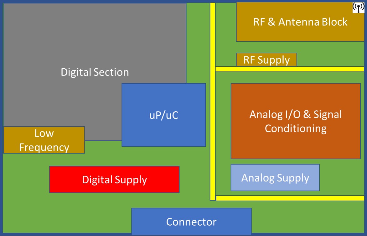
Systematic component placement is crucial in high-speed PCB design. As an initial step, the designer should thoroughly review the schematic and divide it into functional subsections—such as Analog, digital, high-speed, RF, high-current, and power supply circuits—based on their roles within the design. A standard high-speed design flow: –
(Schematic → Floorplanning → Pre-layout SI Analysis → Placement/Routing Adjustments → Final Layout).
Effective component placement is critical in high-speed PCB design to ensure signal integrity and overall board performance. Key strategies include:
- Pre-placement floorplanning helps organize components early, enabling optimal placement of small parts like bypass capacitors and termination resistors.
- Group functional blocks (e.g., Power, RF, Analog, Digital) to minimize signal crossings and noise interference.
- Short signal paths are essential—place components involved in high-speed signal chains close to one another.
- Reserve routing channels and plan for sufficient space during placement to avoid congestion.
- Consider power and ground plane requirements when assigning areas for functional blocks.
- Use continuous power planes where possible; if split planes are necessary, avoid placing high-speed signals across splits to preserve return paths.
- Maintain functional grouping integrity—avoid mixing components from different circuit types to reduce return path disruption and potential EMI issues.
- Avoid placing high-speed components near board edges, as edge impedance variations and EMI susceptibility are higher. Keeping these components near the board center helps reduce EMI impact, especially from nearby connectors.
- Thermal management is critical—high-speed components often run hot. Ensure hot devices like BGAs receive unobstructed airflow, and avoid blocking it with large components such as connectors.
- Termination resistors should be integrated during the initial placement phase—not added as an afterthought. Their placement is crucial for minimizing signal reflections and maintaining circuit integrity.
- Since this is a high-speed design, the termination strategy should be selected based on the specific interface requirements, and components must be placed accordingly. It’s important to note that the initial component placement will serve as the input for pre-layout Signal Integrity (SI) analysis. Based on the results of this analysis, the component placement may need to be adjusted to optimize signal performance.
Incorporating these placement strategies—while also considering routing paths, and power and ground requirements—helps build a robust and reliable high-speed PCB. Ultimately, thoughtful placement improves both signal performance and board manufacturability.
Component Orientation and Placement Strategies
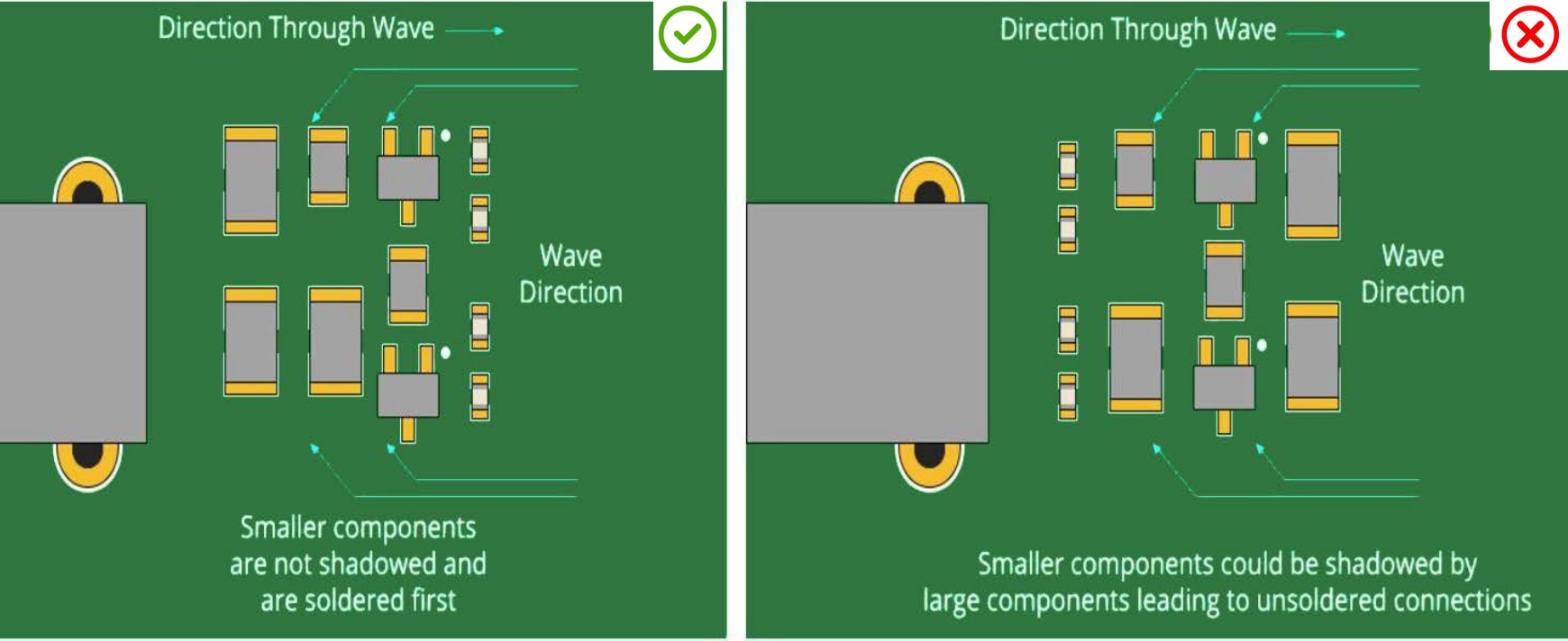
Aligning similar components in the same direction is a key practice in PCB design, as it simplifies routing and supports a smoother, error-free wave soldering process during assembly. It’s generally recommended to place all surface-mount devices (SMDs) on the same side of the PCB, and all through-hole components on the top side to reduce assembly complexity and cost.
Ideal component placement positions smaller components ahead of larger ones in the direction of the solder wave. This allows the wave to reach and solder smaller parts first, avoiding shadowing. If larger components are placed upstream, they can block the wave, leading to unsoldered joints on smaller components. The diagram below illustrates how thoughtful component placement can significantly enhance the assembly process.
Components come in various package types, and some packages may allow for shorter trace lengths, which is beneficial for high-speed performance. Additionally, component footprints should be optimized with thermal management in mind. One effective method for heat dissipation is placing power pads directly beneath ICs and connecting them to internal planes. Even small adjustments in pad shapes can help reduce routing complexity and connection lengths, contributing to a more compact and efficient layout.
Functional Requirements When Placing PCB Components
🔧 Functional PCB Component Placement Guidelines
- Optimize placement for circuit functionality:
-
- Place components where they best support circuit function.
- Ideal pin-to-pin connections are difficult in high-density layouts; placement requires compromises to optimize overall performance.
- Designers must balance compromises for best overall performance.
📌 Component Placement Principles
- General digital component placement:
-
- Fixed Components First: Place connectors, switches, mounting holes, and other position-critical parts.
- High-Speed Components: Position processors, memory, transceivers close to each other to minimize trace lengths.
- Keep each circuitry block separate—allow overlap only for transition components (e.g., ADCs).
- Ensure room for escape/bus routing; don’t block routing channels.
- Plan for signal return paths— avoid via placements that block reference planes.
- For high-speed paths, keep related components close and trace lengths short and direct.
- Analog and power circuitry placement:
-
- Follow similar separation and proximity rules.
- High-power/high-speed ICs (like processors) must have decoupling capacitors placed very close to power pins.
- Group power supply components tightly together to enable short, wide traces.
- Keep power components on the same PCB layer to avoid vias and reduce inductance.
- Thermal management:
-
- Place hot components (e.g., processors) toward the center of the board to aid heat dissipation.
- Avoid clustering power supplies together to prevent localized heat buildup.
- Ensure airflow paths are not blocked by tall components.
- Leave space for heatsinks or other cooling solutions.
High-Speed PCB Layout Design Guide – Summary
High-speed PCB layout design is essential for modern electronics requiring fast data rates and high processing power, typically involving signals above 100 MHz or interconnect lengths significant enough to demand transmission line practices.
This guide outlines critical design considerations, starting with identifying high-speed signals based on rise time and signal wavelength in PCB materials. Proper footprint design minimizes parasitic effects by limiting pad size increases and using rounded corners.
Floor planning should segment the board into functional blocks (digital, analog, RF, power), group components to shorten trace paths, and maintain power/ground continuity while avoiding noisy board edges. Component orientation should support streamlined routing and manufacturability by aligning packages, minimizing thermal stress, and keeping SMDs on the same side.
Placement strategy begins with fixed components, followed by tightly grouped high-speed elements like CPUs and RAM to preserve signal integrity, while analog and power parts benefit from decoupling, minimal vias, and close coupling. Thermal management involves centering hot components, enabling airflow, and isolating heat zones to ensure reliable high-speed performance.
Author Profile
- 20+ years embedded hardware design professional with a burning passion for teaching. Sharing the intricate world of embedded hardware is my mission and joy.
Latest entries
 Tech Updates30 November 2025STM32WBA6: The Next-Generation MCU Powering Secure Short-Range Wireless Designs
 Blogs24 November 2025High-Speed PCB Layout Design Guide-104
 Tech Updates14 September 2025Renesas Launches RL78/L23 Ultra-Low-Power MCUs to Power Smarter Home Appliances
 Blogs7 September 2025High-Speed PCB Layout Design Guide-103