DDR3 SDRAM is 3rd generation of DDR SDRAM Memory, known for synchronous operation, increased data transfer rates, enhanced memory bandwidth, lower power consumption, higher memory density, and compatibility with DDR2 Memory. Featuring a double data rate, and 8n-prefetch architecture, DDR3 enables more efficient data retrieval in a single read operation.
DDR3 memory offers high data transfer rates ranging from 800 to 2133 MT/s, utilizing both rising and falling edges of a 400 to 1066 MHz I/O clock. This signifies a significant improvement over DDR2’s rates (400–1066 MT/s) and a fourfold increase compared to DDR’s rates (200–400 MT/s).
DDR3 SDRAM achieves high-speed operation, approximately twice that of DDR2 SDRAM, while mitigating increased power consumption. This is achieved through the use of a lower voltage of 1.5V for both the power supply and interface. The combination of improved speed and reduced power consumption makes DDR3 a more efficient and advanced memory technology compared to its predecessor, DDR2.
Specification of DDR3 Vs DDR2 SDRAM Memory
|
Parameters |
DDR3 SDRAM |
DDR2 SDRAM |
|
Typical Operating Voltage |
1.5 ± 0.075 V |
1.8 ± 0.1 V |
|
I/O Voltage |
1.5V |
1.8V |
|
Densities |
256Mb–8Gb |
256Mb–2Gb |
|
I/O Width |
x4/ x8/ x16 |
x4/ x8/ x16 |
|
No of Bank |
8 |
4 or 8 |
|
Prefetch Architecture |
8N |
4N |
|
input/output logic level |
STL_15 |
STL_18 |
|
/CAS Latency(CL) |
5, 6, 7 clocks |
3, 4, 5, 6 clocks |
|
Posted CAS, Additive Latency (AL) |
AL = 0/CL – 1/CL – 2clocks |
0, 1, 2, 3, 4 clocks |
|
/CAS write latency |
CAS Latency(CL) |
READ latency – 1 clock |
|
/CAS Read latency |
AL + CWL |
AL + CL |
|
Clock Speed(Internal) |
400/533/667/800MHz |
200, 266, 333, 400 MHz |
|
Data Rate |
800-1600 Mbps |
400-800 Mbps |
|
Burst Length |
4(burst chop)/,8 |
4,8 |
|
Data Strobe |
Differential |
Bidirectional strobe (single ended or differential) with RDQS |
|
ZQ pin Functionality for ODT calibration |
Available. For ZQ Calibration |
NA |
|
Dynamic ODT |
Available |
NA |
|
CLK-DQS de-skewmechanism |
Available (Write levelling, Read levelling) |
NA |
|
/Reset pinFunctionality |
Available |
NA |
|
Package |
FBGA only |
FBGA only |
Functional Block of DDR3 VS. DDR2 SDRAM
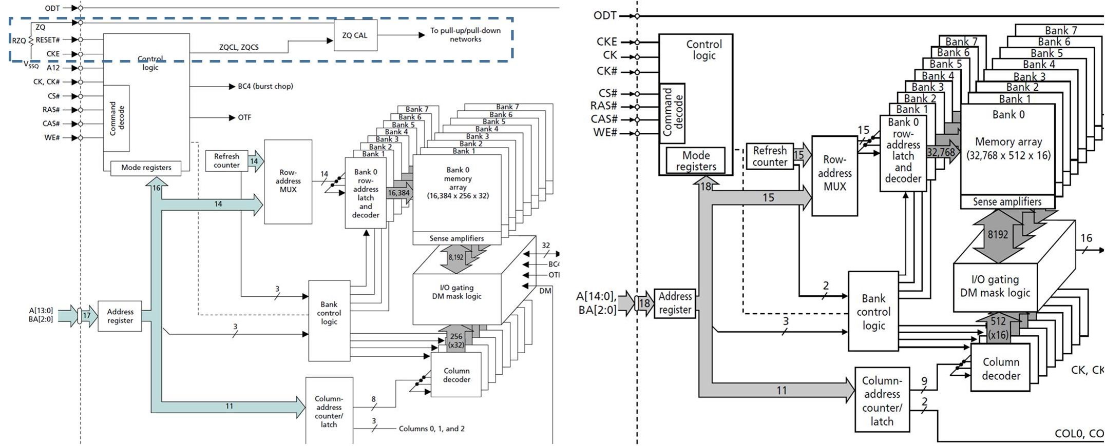
The comparison of the functional block diagrams for the 2Gb, 128 Meg x 16, DDR3 and DDR2 memory indicates a fundamental similarity in the memory core structure, as illustrated in above Figure. Despite potential differences in their operational aspects, the core components and organization of the memory appear to align closely between DDR3 and DDR2 configurations.
We can see major updates in command and Control Block. New features like ZQ Calibration and Reset Pin Functionalityis newly added in DDR3 block as shown in above picture. ZQ calibration is intended to control the on-die termination (ODT) values and output drivers (RTT and RON respectively) of the SDRAM. The new DDR3 architecture also supports a reset pin. This reset pin is designed to allow the user to clear all data (information) stored the DDR3 SDRAM. The advanced benefit of this feature is that, there is no need to RESET each control register separately or restart (power down and up again) each individual DDR3 SDRAM. By initiating a RESET, the DDR3 SDRAM will recover in a known good state (if needed).
New Features of DDR3 SDRAM
Burst length (BL) of DDR3 SDRAM
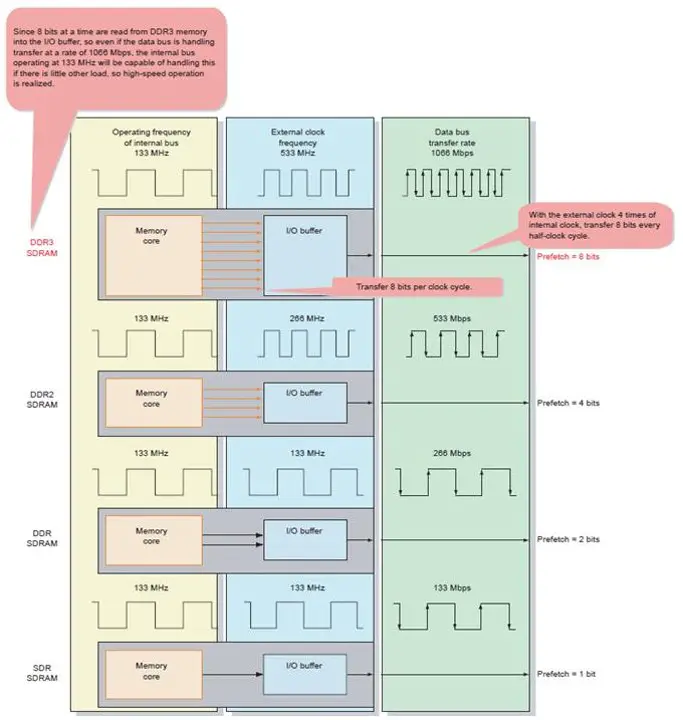
DDR3 SDRAM typically operates with a default burst length (BL) of 8 bits, aligning with its 8-bit Prefetch architecture. However, it also supports a 4-bit burst length, inherited from DDR2 SDRAM. In this configuration, known as Burst Chop Mode (BC4), data is treated as if the second half (four bits) is masked during an 8-bit burst length access, the column command interval (ICCD) becomes 4 times the clock cycle time (4tCK) in connection with the 8-bit Prefetch. This flexibility in burst length configurations allows system designers to optimize memory access based on specific performance requirements.
8-Bit Prefetch Architecture
DDR3 SDRAM employs an 8-bit Prefetch architecture, allowing it to read/write 8 bits of data in parallel from the DDR3 SDRAM core during each operation. The bus width of the DDR3 SDRAM core is eight times wider than the I/O bus width. Hence operating frequency of the DDR3 SDRAM core is set to be 1/8 of the data rate of the I/O interface section. This relationship ensures efficient synchronization and data transfer between the DDR3 SDRAM core and the I/O interface. During a read operation, 8-bit data is read in parallel from the DDR3 SDRAM core. This data is then converted to serial data and output from the I/O pin in synchronization with the clock, utilizing a double data rate. For a write operation, serial data input from the I/O pin, synchronized with the clock at a double data rate, is converted to parallel data. This parallel data, organized as 8-bit data, is then written to the DDR3 DRAM core.
Read Latency (RL) & Write Latency (WL)
Read latency (RL) is the time from issuing a READ command to the output of the first data, while write latency (WL) is the time from issuing a WRITE command to the input of the first data. These latencies are critical timings in DDR3 SDRAM, reflecting the delays in reading and writing operations, and minimizing them is important for optimizing memory access performance.
Legend:-
AL: Additive latency
CL: CAS latency
CWL: CAS write latency
|
PARAMETERS |
DDR3 SDRAM |
DDR2 SDRAM |
|
RL (Read latency) |
RL = AL + CL |
RL = AL + CL |
|
WL (Write latency) |
WL = AL + CWL |
WL = RL – 1 = AL + CL – 1 |
|
CL |
5, 6, 7, 8, 9, 10, (11) |
(2), 3, 4, 5, 6 |
|
AL |
0, CL – 1, CL – 2 |
0, 1, 2, 3, 4, (5) |
|
CWL |
5, 6, 7, 8 |
N/A |
RESET Pin
In DDR3 SDRAM, the /RESET pin is introduced as a new feature. The /RESET pin is utilized by driving it low during power-on, initialization processes, or when a RESET of the memory module is necessary. This pin provides a means to initiate a RESET condition, ensuring proper initialization and configuration of the DDR3 SDRAM module.
DDR3 Leveling
The DDR3 controller has a new feature called leveling to correct command and DQS skew caused by the fly-by topology. It supports full and incremental leveling, but software must enable it after initialization, providing a customizable solution for addressing signal timing issues in memory operations.
Full Leveling (Auto Leveling)
Full leveling, or auto leveling, in DDR3 controllers involves write leveling, read DQS gate training, and read data eye training. Write leveling compensates for command-to-DQS delays in writes, while read DQS gate training determines optimal DQS timing. Read data eye training aligns the valid DQS signal with the center of the DQ line during reads by adjusting the DQS delay relative to DQ. This ensures precise timing for both write and read operations in DDR3 memory systems.
Incremental Leveling
Incremental leveling is a feature designed to monitor voltage and temperature (V-T) variations over time, which may impact the DQS de-skewing process established during full leveling in DDR3 controllers. Following the initial full leveling, periodic incremental leveling can be executed to precisely track V-T drifts and maintain optimal signal alignment. This feature provides good control over specific leveling types, including write, read DQS gate, and read data eye, ensuring ongoing accuracy in compensating for environmental changes in DDR3 memory systems.
ZQ Calibration
DDR3 Synchronous Dynamic Random-Access Memory (SDRAM) employs the ZQ calibration function instead of the On-Chip Driver (OCD) function. ZQ calibration is a process used to calibrate the impedance of the memory module, ensuring optimal signal integrity and performance. Unlike the OCD function, which focuses on controlling the output driver impedance, DDR3 SDRAM relies on ZQ calibration for impedance adjustments, contributing to improved stability and reliability in memory operations.
During ZQ calibration, the DDR3 SDRAM memory controller sends a calibration command to the memory module, instructing it to adjust the impedance of the entire memory module, not just the output driver impedance to a specified target value. It ensures that the input and output impedances of the memory module are at the desired values. By fine-tuning the impedance of the memory module, ZQ calibration contributes to stable and reliable data transfers.
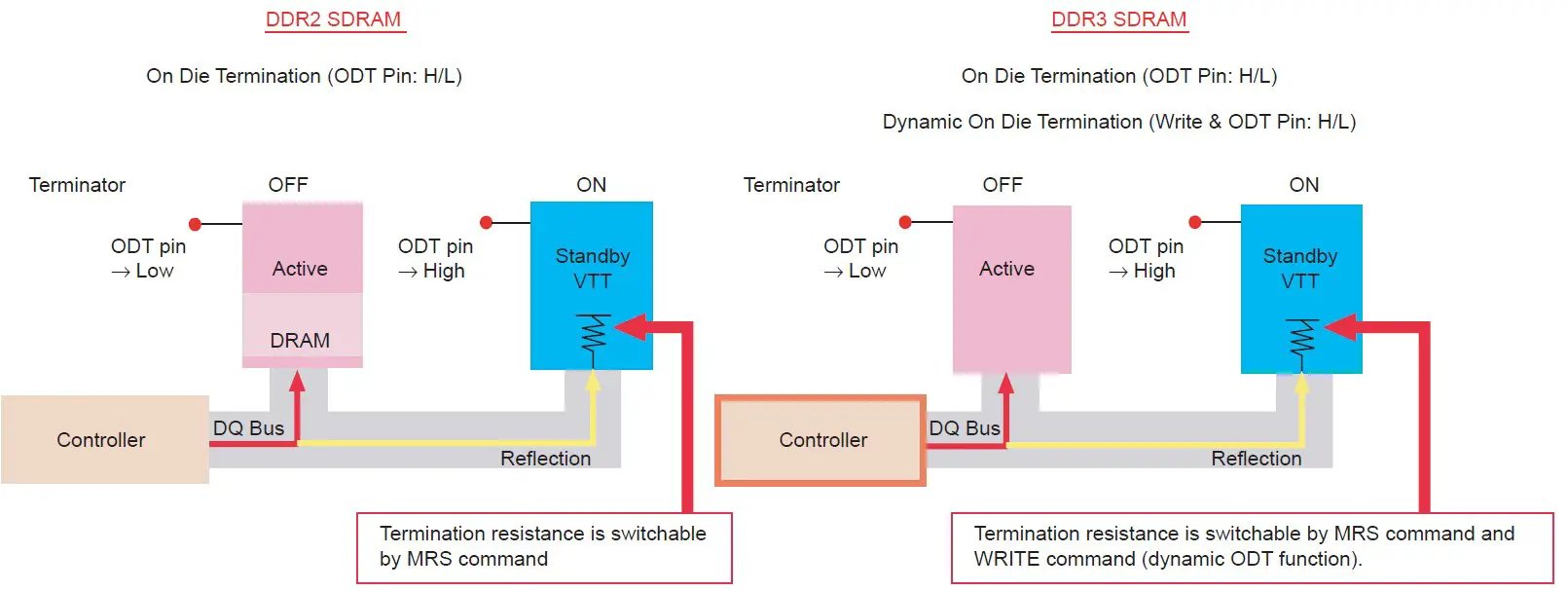
Dynamic ODT (Dynamic On-Die Termination)
DDR3 SDRAM technology can transfer data at a much higher rate than previously possible. With these improved data rates, designers need options to improve the signal integrity of the data bus, while still maintaining performance. DDR3 SDRAM inherits the ODT function from DDR2 and introduces a dynamic ODT mode. In dynamic ODT, the impedance of the termination resistor can be dynamically varied in response to changes in data patterns, frequency, or temperature. This function allows dynamic switching of ODT resistance during WRITE operations without the need for a Mode Register Set (MRS) command. Dynamic ODT helps in optimizing termination under varying conditions, enhancing signal integrity and system performance.
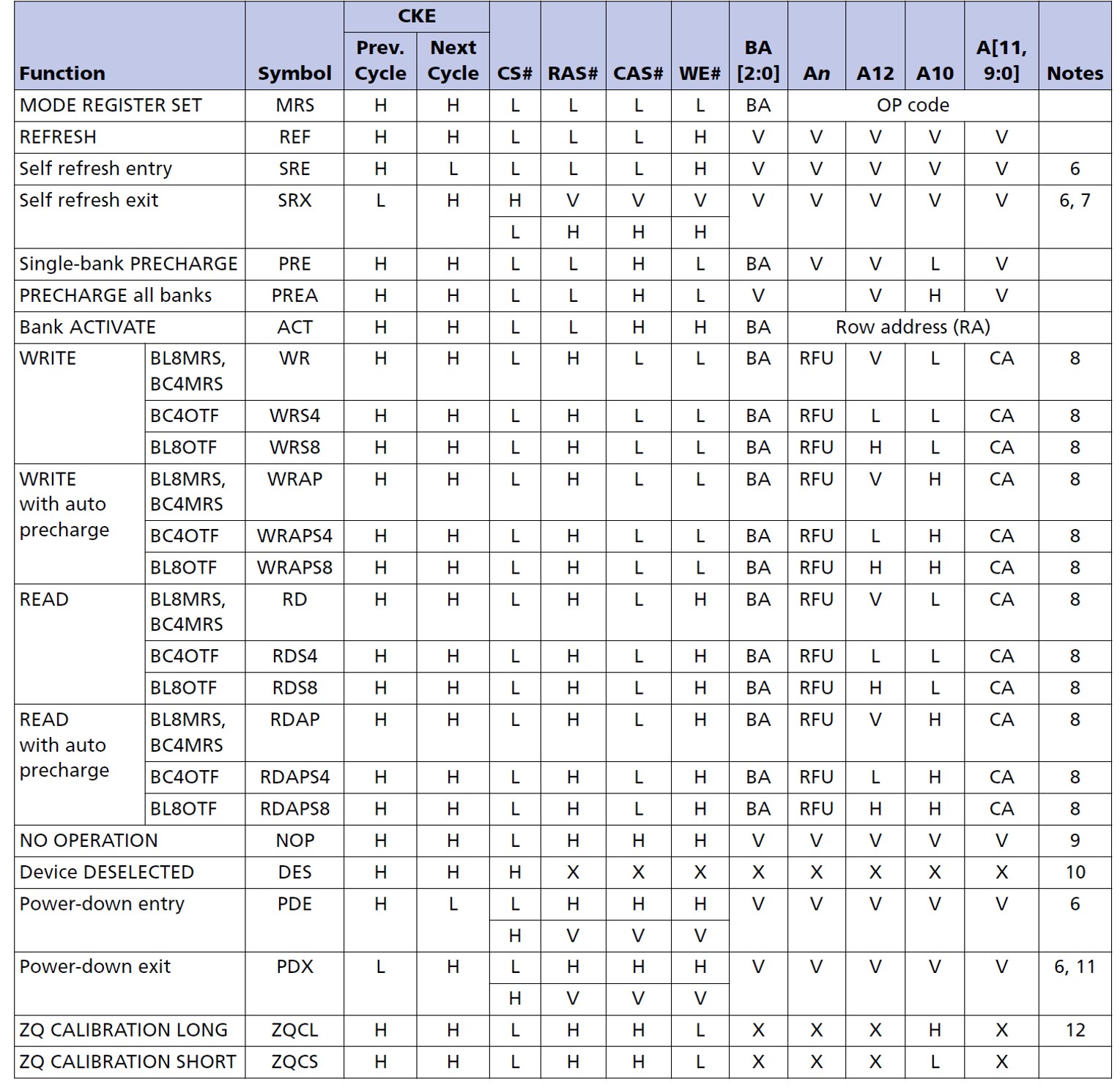
DDR3 SDRAM Commands
In DDR2 SDRAM (Double Data Rate Synchronous Dynamic Random Access Memory), the memory controller communicates with the memory module by issuing commands at the rising edge of the clock signal (CK) and is defined by the states of CS#, RAS#, CAS#, WE#, and CKE.
The rising edge of the clock signal is used as a reference point for the timing of commands and data transfers. This synchronous operation ensures that data is transferred and commands are executed in a coordinated manner, enhancing the overall efficiency and reliability of the memory system.
DDR3 SDRAM (Synchronous Dynamic Random-Access Memory) commands and their meanings are provided as below. These commands are essential for controlling the operation and data access of DDR3 SDRAM devices. Here’s a summary of these commands and their functions:
Summary
- DDR3 Key Features
- Double Data Rate (DDR) with 8n-prefetch architecture for more efficient data retrieval.
- Data transfer rates ranging from 800 to 2133 MT/s.
- Utilizes both rising and falling edges of a 400 to 1066 MHz I/O clock.
- Lower voltage of 1.5 V for both power supply and interface, reducing power consumption.
- Significant improvement in speed compared to DDR2, approximately twice as fast.
- Specifications Comparison (DDR3 vs. DDR2)
- Operating Voltage: DDR3 (1.5 V), DDR2 (1.8 V)
- Densities: DDR3 (256Mb–8Gb), DDR2 (256Mb–2Gb)
- Prefetch Architecture: DDR3 (8N), DDR2 (4N)
- CL (CAS Latency): DDR3 (5, 6, 7 clocks), DDR2 (3, 4, 5, 6 clocks)
- Burst Length: DDR3 (4/8), DDR2 (4, 8)
- Data Rate: DDR3 (800-1600 Mbps), DDR2 (400-800 Mbps)
- ZQ Pin Functionality for ODT Calibration: Available in DDR3, Not Applicable in DDR2
- Dynamic ODT: Available in DDR3, Not Applicable in DDR2
- Functional Comparison:
- Similarity in the core structure of DDR3 and DDR2 memory despite operational differences.
- Introduction of new features in DDR3, such as ZQ Calibration and Reset Pin Functionality.
- New Features of DDR3 SDRAM
- Burst Length (BL) flexibility, supporting both 8-bit and 4-bit configurations.
- 8-Bit Prefetch Architecture for efficient data transfer.
- DDR3 Leveling for command and DQS skew correction.
- ZQ Calibration for on-die termination (ODT) values and output driver control.
- Dynamic ODT for dynamically varying termination resistor impedance.
- /RESET pin for initiating a reset condition in DDR3.
Author Profile
- 20+ years embedded hardware design professional with a burning passion for teaching. Sharing the intricate world of embedded hardware is my mission and joy.
Latest entries
 Tech Updates30 November 2025STM32WBA6: The Next-Generation MCU Powering Secure Short-Range Wireless Designs
 Blogs24 November 2025High-Speed PCB Layout Design Guide-104
 Tech Updates14 September 2025Renesas Launches RL78/L23 Ultra-Low-Power MCUs to Power Smarter Home Appliances
 Blogs7 September 2025High-Speed PCB Layout Design Guide-103