Ethernet is essential in various applications due to its speed and reliability. It forms the backbone of office LANs and data centers, provides stable internet and home automation connectivity, and supports industrial automation and SCADA systems. Today’s most common Ethernet speeds are 100 Mbps, 1,000 Mbps, and 10 Gbps.
For PCB designers, Ethernet layout routing is a formidable challenge due to the increasing demand for high-speed Ethernet. Even at the lowest rate, careful PCB layout design is crucial to ensure reliability and performance. Significant challenges for routing GbE Ethernet includes Ensuring spacing between differential pairs, Maximizing signal strength, Isolation of different signal types and Achieving electromagnetic compatibility(EMC).
By following proper guidelines, PCB designers can effectively manage the challenges of routing high-speed Ethernet signals, ensuring reliable and high-performance network connectivity.
Ethernet Component Placement
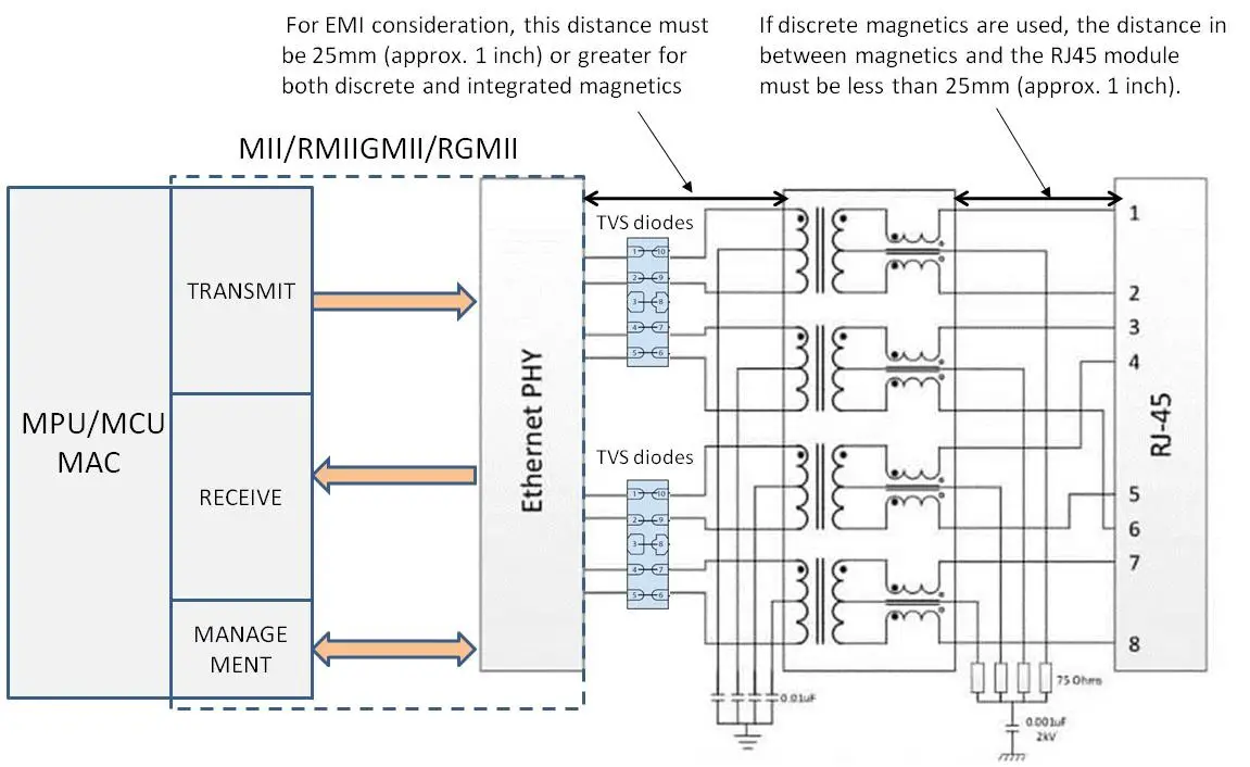
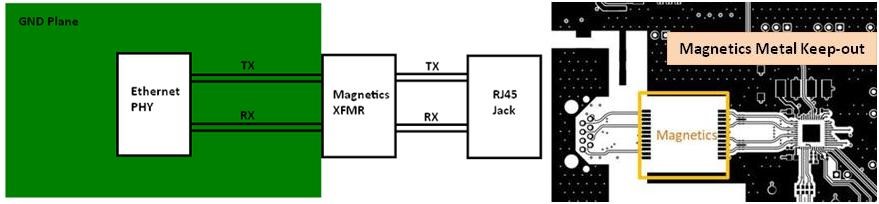
All the components of the Ethernet interface are shown in the picture below. In this article, we will try to understand the placement & routing guiltiness of all these components. We will also try to understand the layer stack-up for the Ethernet interface and explore specific guidelines related to MII, RMII, GMII, and RGMII for Ethernet interfaces.
Decoupling Capacitors
- Place decoupling capacitors as close to the PHY as possible.
- Typically, the smallest capacitors (e.g., 0.01 µF, 0.1 µF) should be closest to the PHY. Larger capacitors (e.g., 1 µF, 10 µF) are usually placed slightly farther away.
- Verify specific recommendations in the device data sheet. Follow any pin-specific guidelines from the data sheet.
Clock Source
- Place the oscillator close to the PHY to minimize PLL noise and ensure spec-compliant behavior.
- A crystal should only drive one device and never multiple devices.
- Reference the relevant application note for detailed crystal placement and design guidelines.
- Must be routed over a continuous ground plane. It should not be routed across any plane splits or traces on adjacent layers.
Magnetics Placement Guidelines
- If the magnetic is a discrete component, then it should be placed no greater than 1 inch away from the Ethernet jack.
- The distance between the Ethernet PHY and the magnetic should be 25mm (1 in.) or greater. The 1 in. design rule is considered good design practice among PHY vendors to isolate the PHY from the magnetics.
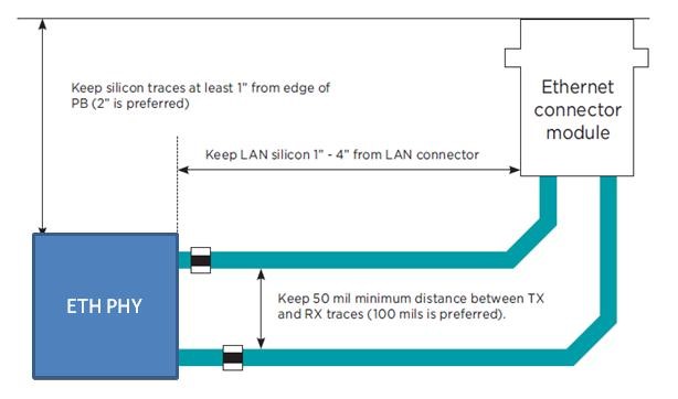
- Keep the PHY device and the differential TX/RX pairs at least 1 inch from the edge of the PCB, up to the magnetics.
- For an integrated magnetics Ethernet jack, the differential pairs should be routed to the back of the integrated jack, away from the board edge.
- Refer to below Figure for some basic placement distance guidelines. Although it shows two differential pairs, it can be generalized for 1000BASE-T to 10GBASE-T systems with four analog pairs. The ideal placement for the Ethernet silicon would be approximately one inch behind the Ethernet magnetic.
Termination Resistors Placement Guidelines
- The 49.9 ohm pull-up resistors on RX/TX should be placed as close as possible (within 400 miles) of the Ethernet PHY and should be placed next to the RX/TX pairs to minimize stubs. This also ensures similar RX/TX transmit paths.
- Place a 0.01 µF decoupling capacitor for each channel between 2.5V plane and ground close to the termination resistor. Place a 0.01 µF decoupling capacitor for each port at the transformer center tab.
Ethernet Routing Guidelines
PCB Layer Stacking
A minimum of four PCB layers is necessary for Ethernet routing. To meet performance requirements, a six -Layer board design is recommended. The following is the layer stacking recommendations for four, six, and eight-layer boards.
Four-layer board :
- Signal 1 (top layer)
- GND
- 3.3 Volt power plane
- Signal 2, planes for 1.8 Volt and 2.5 Volt
Six-layer board:
- Signal 1 (top layer)
- Power plane
- Signal 2 (best for clock and MDI signals)
- Signal 3 (best for clock and MDI signals)
- GND
- Signal 4
Eight-layer board:
- Signal 1 (top layer)
- GND
- Signal 2 (best for clock and MDI signals)
- Power plane 1
- GND
- Signal 3 (best for clock and MDI signals)
- GND or power plane 2
- Signal 4
MDI Signals (Tx+/Tx- and Rx+/Rx-) Routing
- Keep the traces between the magnetic module and the RJ-45 jack as short as possible. Each MDI trace should be less than 2 inches (2000 mils) in length.
- Route MDI traces to transformer on the same layer.
- The individual trace impedance of Tx+/Tx- and Rx+/Rx- must be kept below 50W. Maintain a typical impedance of 100Ω differential with ±10% control.
- The Tx+/Tx- and Rx+/Rx- traces should always be as short as possible (less than 25 mm or 1″). If longer traces are absolutely required, the maximum length is limited to 75 mm (3″).
- Route each Tx+/Tx- and Rx+/Rx- pair together, keeping their separation under 0.25 mm (0.01″), using 0.25 mm (0.01″) traces.
- Keep the Tx+/Tx- and Rx+/Rx- trace lengths as equal as possible (Within 5 mils).
- The separation between the Tx+/Tx- and the Rx+/Rx- differential pairs must be at least 0.5 mm(0.02″). It is best to separate them with a ground plane.
- Length Matching:
- For 1G transmission, traces should be length-matched within 20 miles.
- For 100M or 10M transmissions, traces should be length-matched within 50 miles.
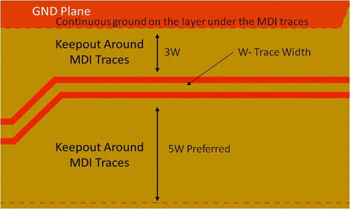
- Ground Plane Distance: Designing with proper distance between the MDI trace and the ground plane prevents unwanted capacitive impedance.
- Minimum Distance: If w equals the width of the MDI trace, ground planes on the same layer should be distanced at least 3 times the width of the MDI trace (3*w).
- Preferred Distance: The preferred distance is 5 times the width of the MDI trace (5*w).
- Continuous Ground: It is recommended to have a continuous ground plane on the layer under the MDI traces as shown in below picture.
- Void under Components: Ground plane should be cut or voided only under specific components on the trace, such as transformers/magnetics, chokes, AC coupling capacitors, and ESD diodes.
- Automotive Applications: For automotive applications, an all-layer void is ecommended, but at minimum, a two-layer void is required. This includes voiding the layer the component is on and the layer directly below it.
- Standard Applications: For standard applications, a two-layer void is also recommended.
MII Signals (MII, RMII, GMII, and RGMII) General guidelines
- Total Length: Keep MII signals short and direct. Ideally, limit the length to 6 inches or less to avoid significant signal degradation Length Matching:
- Ensure that data lines (TXD, RXD) are length-matched to the respective clock signals.
- For 1G transmission, RX and TX traces should be length-matched within 20 miles.
- For 100M or 10M transmissions, RX and TX traces should be length-matched within 50 mils.
- RX traces must be length-matched to each other, and TX traces must be length-matched to each other.
- Termination: Series termination resistors (typically 22Ω to 33Ω) may be required at the source to reduce reflections.
- Vias and Stubs: Minimize the number of vias and stubs on MII traces to reduce signal degradation.
- Single-Ended Impedance: Maintain a single-ended impedance of 50 Ohms with a tolerance of +/- 10%. Ensure impedance matching to prevent signal reflections and loss.
- Ground Keep Out:
- Minimum Distance: Maintain a ground keep-out area around MII traces that is at least 3 times the width (w) of the trace.
- Preferred Distance: Ideally, the ground keep-out area should be 5 times the width (w) of the trace to minimize interference and capacitive coupling.
Interface Specific Guidelines
|
Interface |
Parameters |
Layout Recommendations |
|
MII |
Clock Signal |
MII interfaces typically consist of clock (TX_CLK and RX_CLK) and data pairs (TXD[0:3] and RXD[0:3]). Clock Speed 25MHz |
|
|
Length-matching |
Each data pair (TXD[i] and RXD[i]) should be length-matched with respect to its corresponding clock signal (TX_CLK and RX_CLK). A common guideline is to keep the length difference within ±0.5 inches (±12.7 mm) |
|
RMII |
Clock Signal |
RMII uses a single 50 MHz reference clock (REF_CLK) shared between the MAC and PHY. Ensure low jitter and minimal skew. Clock skew for RX and TX paths can be optimized independently. |
|
|
Length-matching |
Length-matching of data lines (TXD[1:0], RXD[1:0]) to the reference clock (REF_CLK) is crucial. Skew between TXD[3:0] lines must be less than 11ps, which correlates to 60 mil for standard FR4. Skew between RXD[3:0] lines must be less than 11ps, which correlates to 60 mil for standard FR4. A common guideline is to keep the length difference within ±0.5 inches (±12.7 mm) |
|
GMII |
Clock Signal |
GMII requires two clocks: GTX_CLK (for transmit) and RX_CLK (for receive). Ensure both clocks are low jitter and properly matched with their respective data signals. Clock Speed 125MHZ. |
|
|
Length-matching |
Differential pairs and data signals (TXD[7:0], RXD[7:0]) should be length-matched to their respective clocks. Length differences should be within 50 mils (1.27 mm). |
|
|
Termination Resistor |
The rise and fall times of GMII are in the order of 500 ps for RX_CLK, and GTX_CLK. Propagation Delay = 170 ps/inch on a FR4 board. Equivalent length of rise time = (1/6) Rise time (ps) / Delay (ps/inch) = (1/6) *(500/ 170) = 0.5 inch. Thus, series termination is not needed for traces less than 0.5 inch long. Trace monger than 0.5 Inch need termination resistors. |
|
RGMII |
Clock Signal |
Clock and Data Pairs: RGMII interfaces consist of clock (TXC and RXC) and data pairs (TXD[0:3], TXCTL, RXD[0:3], RXCTL). Clock Speed 125MHZ with double data rate transmission. |
|
|
Length-matching |
Each data pair should be length-matched with respect to its corresponding clock signal: TXC to TXD[i] (for Transmit data lanes) RXC to RXD[i] (for Receive data lanes). Length differences should be within 20 mils.
|
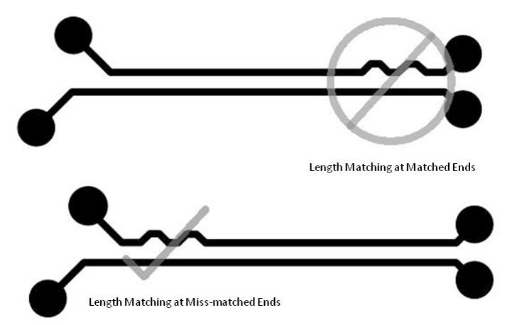
Signal Length Matching
To match the trace lengths, different routing techniques can be used. It is recommended to apply those techniques on the same end of the length-matched pair. The figure below shows the difference between mismatched length-matching and matched length-matching.
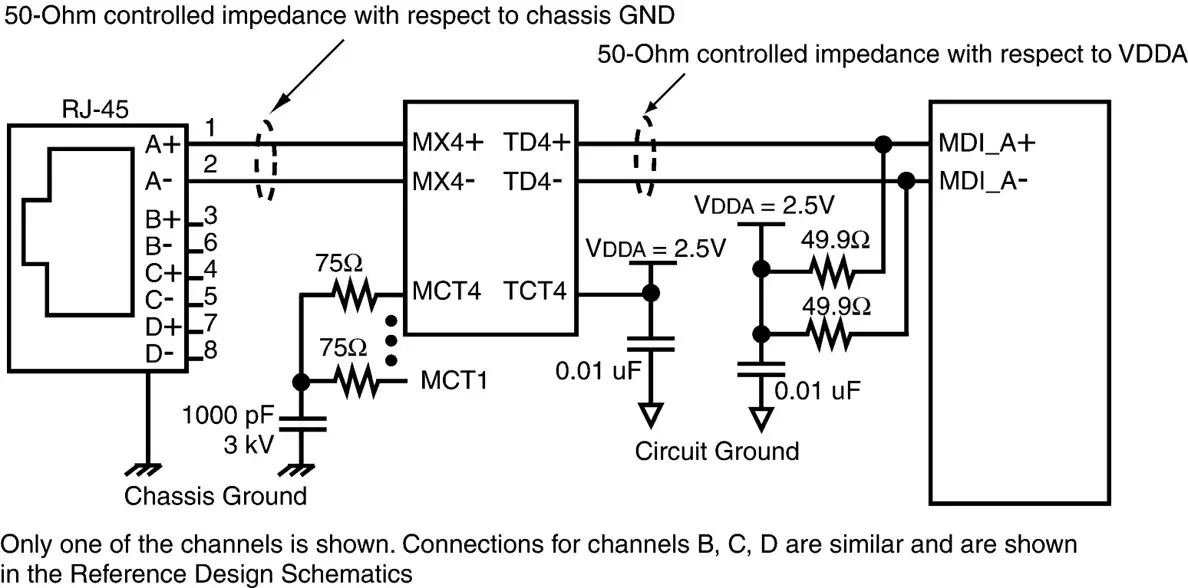
Ethernet Jacks and Magnetics
Discrete magnetics module
- If using a discrete magnetics module, a ground plane must not be placed under the magnetics, the RJ45 connector, or the area between the magnetics and RJ45 connector.
- Metal under the RJ45 connector with integrated magnetic is allowed.
- A ground plane should be placed underneath the RX and TX pairs between the Ethernet PHY and magnetics module as shown below.
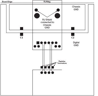
RJ45 Jack with Integrated Magnetics
- A ground plane should be placed under the TX/RX pairs between the Ethernet PHY and Integrated RJ45 jack.
- A separate Ethernet chassis ground should be placed under the RJ45 jack.
- The chassis ground should be connected to the rest of the PCB GND with capacitor stuffing options, which is useful for determining which values and location will provide the best EMI performance. An example drawing is shown below.
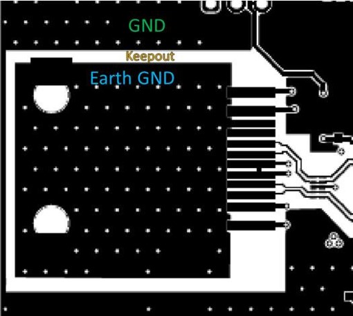
Earth Ground Isolation Guidelines
- Isolation Distance: Earth ground should be isolated from the rest of the board by at least a 20 mil keep-out on all layers.
- Connection Exception: These guidelines ensure proper earth ground isolation while providing a controlled path for potential differences between earth ground and normal ground.
- Earth ground and normal ground should be connected using a capacitor and a high-value resistor.
- A resistor of 1 MΩ or more is recommended for this connection.
- Refer to a typical layout diagram below to visualize this isolation and connection.
ESD and EMI
The following recommendations are provided to help improve ESD & EMI performance:
- Ideally, the PCB design should use 6 or more layers, with solid power and ground planes. With 4 layers, ESD immunity and radiated emissions performance may be compromised.
- To maximize ESD performance, the designer should consider selecting an RJ45 module without LEDs. This will simplify routing and allow greater separation in the Ethernet front end to enhance ESD/susceptibility performance
- To maximize ESD performance, the designer should consider selecting a discrete transformer as opposed to an integrated magnetic/RJ45 module. This may simplify routing and allow greater separation in the Ethernet front end to enhance ESD/susceptibility performance
- When using discrete magnetics, it is critical to use termination: four 75 Ohm for cable-side center taps and unused pins to EFT (Electrical Fast Transient) capacitors.
- Use an EFT capacitor connected to the ground plane and 75 Ohm terminations. Suggested values are 1500 pF/ 2KV or 1000 pF/3KV.
- Use a metal shielded RJ-45 connector, and connect the shield to chassis ground.
- Use magnetics with integrated common mode choking devices.
- Do not overlap the circuit and chassis ground planes, keep them isolated. Connect chassis ground and system ground together using two size 1206 zero ohm resistors across the void between the ground planes on either side of the RJ-45. These resistors can be removed or replaced with alternative components (that is, capacitors or EMI beads) during system level certification testing if necessary.
Summary
Ethernet Routing Guidelines:
- Layer Stacking:
- Four-layer board: Signal 1 (top layer), GND, 3.3V power plane, Signal 2 (bottom layer).
- Six-layer board: Signal 1 (top layer), Power plane, Signal 2 (best for clock and MDI signals), Signal 3 (best for clock and MDI signals), GND, Signal 4 (bottom layer).
- Eight-layer board: Signal 1 (top layer), GND, Signal 2 (best for clock and MDI signals), Power plane 1, GND, Signal 3 (best for clock and MDI signals), GND or Power plane 2, Signal 4 (bottom layer).
- MDI Signals (Tx+/Tx- and Rx+/Rx-):
- Keep traces short (less than 2 inches ideally).
- Route MDI traces to the transformer on the same layer.
- Maintain differential impedance (100Ω differential, ±10% tolerance).
- Keep trace pairs close (under 0.25 mm separation).
- Length match within specified tolerances (e.g., ±20 mils for 1G transmission).
- MII Signals (MII, RMII, GMII, RGMII):
- Keep trace lengths short and direct (6 inches or less recommended).
- Ensure proper length matching between data lines (TXD, RXD) and clock signals.
- Implement termination resistors (typically 22Ω to 33Ω) as needed.
- Maintain single-ended impedance of 50 Ohms with ±10% tolerance.
- Provide sufficient ground keep-out areas around MII traces (at least 3 times trace width).
- Clock and Data Pair Routing (e.g., RGMII):
- Length-match clock (TXC, RXC) to data pairs (TXD, RXD).
- Keep length differences within specified tolerances (e.g., ±20 mils for RGMII).
- Ensure differential pairs (TXD, RXD) are properly routed and matched to clocks (TXC, RXC).
- Component Placement:
- Place decoupling capacitors close to PHY (0.01 µF, 0.1 µF closest, larger capacitors slightly farther).
- Oscillator (crystal) should be close to the PHY, not shared between multiple devices.
- Magnetics should be placed within recommended distances from Ethernet PHY and jack.
- Termination resistors (49.9 ohms) should be close to PHY and adjacent to TX/RX pairs.
- EMC Considerations:
- Use a continuous ground plane under MDI traces.
- Ensure proper isolation and connection of chassis ground and system ground.
- Consider shielding and EFT capacitors for ESD and EMI protection.
- Avoid overlaps between circuit and chassis ground planes.
Author Profile
- 20+ years embedded hardware design professional with a burning passion for teaching. Sharing the intricate world of embedded hardware is my mission and joy.
Latest entries
 Tech Updates30 November 2025STM32WBA6: The Next-Generation MCU Powering Secure Short-Range Wireless Designs
 Blogs24 November 2025High-Speed PCB Layout Design Guide-104
 Tech Updates14 September 2025Renesas Launches RL78/L23 Ultra-Low-Power MCUs to Power Smarter Home Appliances
 Blogs7 September 2025High-Speed PCB Layout Design Guide-103