What is SDR SDRAM Memory?
SDR SDRAM stands for “Single Data Rate Synchronous Dynamic Random-Access Memory.” SDR SDRAM was an early type of SDRAM that transferred data on the rising edge of the clock signal, allowing for one data transfer per clock cycle. It had a relatively lower data transfer rate compared to later SDRAM types like DDR (Double Data Rate) SDRAM, making it more suitable for older computer systems with less demanding memory requirements. SDR SDRAM is indeed considered outdated and has been largely replaced by more advanced and faster DDR SDRAM technologies, such as DDR, DDR2, DDR3, DDR4, and DDR5, which offer increased data transfer rates and improved performance for modern computing needs.
Specification of SDR SDRAM Memory
| Parameters | Value |
| Typical Operating Voltage | 3.3V |
| Prefetch Architecture | 1N |
| input/output logic level | LVTTL-compatible |
| CAS Latency | 2-3 Clock cycle |
| Clock Speed | 66 MHz, 100 MHz, 132 MHz, 166 MHz |
| Data Rate | 100-166 MT/s |
| Clock input | Single Clock (Rising edge) |
| Burst Length | 1, 2, 4, 8, full page |
| Data Strobe | Unsupported |
SDR SDRAM Memory Signal Definition
| Signal Name | Descriptions | Active Level | Directions(From SDRAM Controller) |
| CLK | System Clock | On rising edge | Output |
| CKE | SDRAM Clock Enable | High | Output |
| CS | SDRAM Controller Chip Select | Low | Output |
| BA[1:0] | Bank Select Signals | – | Output |
| RAS | Row Signal | Low | Output |
| CAS | Column Signal | Low | Output |
| WE | SDRAM Write Enable | Low | Output |
| D[31:0] | Data Bus | – | I/O |
| A[12:0] | Address Bus | – | Output |
| DQM | Data Mask | Output |
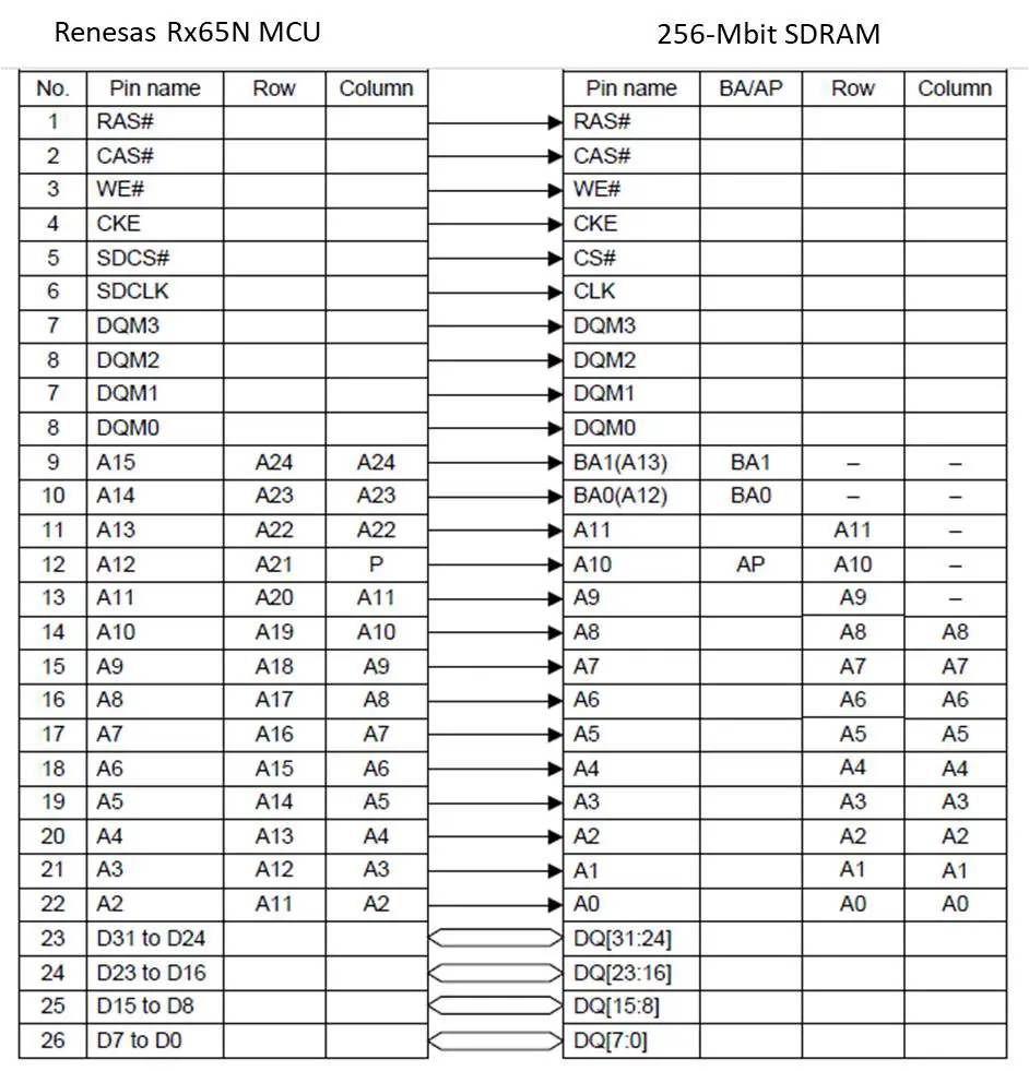
SDR SDRAM Electrical Interface
An example of interfacing a 256-Mbit SDR SDRAM with Renesas Rx65N MCU with 12-bit row address, 9-bit column address and 32-bit bus.
SDR SDRAM Memory Signal Descriptions
Single Data Rate Synchronous Dynamic Random Access Memory (SDR SDRAM) devices use several signals for control and data transfer. Few of the key SDR SDRAM are as below:-
CLK (System Clock): SDRAM Clock Output, rising edge. This is the primary clock signal from the SDRAM controller that controls the timing and synchronizes the operation of all SDRAM operations. All input signals are sampled on the positive edge (ring edge) of this clock signal.
CKE: – SDRAM Clock Enable. CKE acts as an inhibit signal for SDRAM. When a valid read, write, or precharge command is issued, CKE is typically high. When CKE goes low, it signifies that the SDRAM device is entering a power-down mode. Like power-down mode, CKE goes low when the SDRAM device enters self-refresh mode.
CS (Chip Select): The Chip Select signal is used to enable(sampled LOW) or disable (sampled 1GH) the SDRAM device. When active (typically low), command input is valid & SDRAM responds to commands and data. Whenthe CS signal is high, all commands are ignored but the operation continues.
DQ [31:0] (Data In/Out): The DQ input/output Data Bus signals for reading from and writing to the memory are synchronized with the positive edges of CLK. The IOs are byte-maskable during Reads and Writes
A(n:0)- Address bus A(n:0) are sampled during the ACTIVE command and READ/WRITE command with A10 defining auto precharge to select one location out of the memory array in the respective bank. The number of address lines than need to be sampled depends upon memory configurations 4-Bits, 8-Bits, 16-Bits, or 32-Bits, with which memory is interfaced with a processor. A10 is sampled during a PRECHARGE command to determine whether all banks are to be recharged (A10 HIGH) or the bank selected by BA (1.0) [A1 LOW).
DOM (Data Mask): Data Mask signals are issued by SDRAM controller to the memory, sampled during a write cycle and are used to mask data bytes and allow selective writing specific bytes or words within a larger data width. For memory, it is an input mask signal for write accesses and an output enable signal for read accesses.For example, 32-bit SDRAM will have DOM (3:0). DQM3 masks DQ31-0024 DQM2 masks DQ23-0016, DQM1 masks DQ15-DQ8, and DQM0 masks DQ7-DQ0
CAS (Column Address Strobe): The Column Address Strobe CAS# is an active low command signal issued by the SDRAM controller to SDRAM Memory. It is issued within conjunction with the RAS# and signals and is latched at the positive edges of CLK. Different signal levels of RAS, CAS. WE and CS SDRAM controller issues different types of commands to SDRAM to perform different operations.
For example, when RAS is held “HIGH” and CS# is asserted “LOW,” the column access is started by asserting CAS# “LOW.” Then, the Read or Write command is selected by asserting WE# “LOW” or “HIGH”
RAS (Row Address Strobe):The row address strobe RAS# is an active low command signal issued by SDRAM controller to SDRAM Memory. It is issued in conjunction with the CAS# and WE signals and is latched at the positive edges of CLK. Different signal levels of RAS, CAS. WE and CS SDRAM controller issues different type of commends to SDRAM to perform different operations.
For Example, When RAS# and CS# are asserted “LOW and CAS is asserted “HIGH” either the BankActivate command or the Precharge command is selected by the WE signal When the WEB is asserted “HIGH,” the BankActivate command is selected and the bank designated by BA is turned on to the active state. When the WEP isasserted “LOW,” the Precharge command is selected and the bank designated by BA is switched to the idle state after the precharge operation.
WE (Write Enable): The Write Enable signal WE is an active low command signal issued by SDRAM controller to SDRAM Memory. It is issued in conjunction with RAS and CAS signals and is latched at the positive edges of CLX. The WEB input is used to select the BankActivate or Precharge command and Read or Write command.
BAn (Bank Address): The Bank Address issued by SDRAM controller to SDRAM Memory. These signals specify which bank within the SDR SDRAM is being accessed Multiple banks are common in SDR SDRAM devices, and these signals select the appropriate bank. For example two signals BAO, BA1 can select 4 banks by 4 differentlogic level combinations possibility on these signals.
SDRAM Addressing
SDR SDRAM uses a specific addressing scheme that involves selecting both a row and a column to access a particular memory cell within the module. The first step in accessing data from SDR SDRAM is selecting the row that contains the desired memory cell. This row address specifies one of the many rows within the memory bank.After activating the appropriate row, the next step is to select thespecific column within that row. The column address specifies which memory cell within the activated row is to be read from or written to.
By specifying both the row and column addresses, the exact memory address location can be located and data can be accessed within the SDRAM module. This dual-addressing approach is used to access data efficiently and synchronously, allowing for precise and predictable memory operations in line with the system clock.
SDR SDRAM Memory organization and Size
Let’s understand the size of the SDR SDRAM with 64- ROW houses, where each house has 32- person staying in it. Try to calculate the total number of people staying. In the below picture on left hand side 64 X64 houses matrix can be seen and on right hand side we can see the 4 such banks of houses.
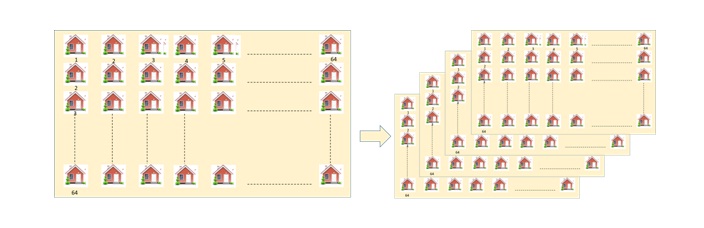
Let’s understand the size of the SDR SDRAM with 64- ROW houses, where each house has 32- person staying in it. Try to calculate the total number of people staying. In the below picture on left hand side 64 X64 houses matrix can be seen and on right hand side we can see the 4 such banks of houses.
Total number of houses in one bank= 64 x64 = 4096 House locations
Total number of houses in 4 such bank= 4096 x4 = 16384 House locations
Total number of people in 16384 Houses (32-People per house) = 16384 x32= 5, 24,288 People.
If we resemble a house example with SDR SDRAM memory, we will have 16384 memory locations (including 4-Banks) in memory. 32 people per house resemble 32- bit of SDR SDRAM memory, where each location is capable of storing 32-bit. Hence the size of this SDR SDRAM will be 5, 24,288- Bits or 512- Bytes.
16-Bits SDR SDRAM Memory
In the case of 16 bits of SDR SDRAM Memory number of Memory locations will be simply doubled in comparison of 32-bit wide memory. Hence calculation will be as below.
Total number of houses in 4 such bank= 16384 x2 = 32768 House locations, which resemble total memory location (including 4-Banks) in a memory
Total number of people in 65536 Houses (16-People per house) = 32768 x16= 5, 24,288 People.
Hence the size of this SDR SDRAM will remain the same as 5, 24,288- Bits or 512- Bytes.
8-Bits SDR SDRAM Memory
In the case of 8 bits of SDR SDRAM Memory number of Memory locations will be simply doubled in compare of 16-bit wide memory. Hence calculation will be as below.
Total number of houses in 4 such bank= 32768 x2 = 65536 House locations, which resemble total memory location (including 4-Banks) in a memory
Total number of people in 65536 Houses (16-People per house) = 65536 x 8= 5, 24,288 People.
Hence the size of this SDR SDRAM will remain the same as 5, 24,288- Bits or 512- Bytes.
4-Bits SDR SDRAM Memory
In the case of 4 bits of SDR SDRAM Memory number of Memory locations will be simply doubled in compare of 8-bit wide memory. Hence calculation will be as below.
Total number of houses in 4 such bank= 65536 x2 = 131072 House locations, which resemble total memory location (including 4-Banks) in a memory
Total number of people in 65536 Houses (16-People per house) = 131072 x 4= 5, 24,288 People.
Hence the size of this SDR SDRAM will remain the same as 5, 24,288- Bits or 512- Bytes.
Functional Block Diagrams of 256Mb SDR SDRAM
64 Meg x 4 Functional Block Diagram
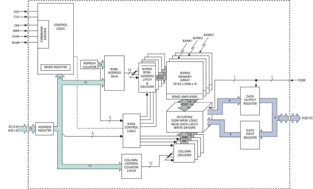
Memory calculations for above memory SDR SDRAM organizations:-
Data Bus Width = 4-Bits
No of Row Address Bits: – 13
No of Column Address Bits: – 11
No of Banks = 4
Total number of Memory locations in the SDR SDRAM=
2^No of Row Address Bits x 2^ No of Column Address Bits x No of Banks
= 2^13 x 2^ 11 x 4 = 2^13 x 2^ 11 x 2^2 = 2^26 =64 Mega locations
Total Size of SDR SDRAM memory =
Data Bus Width x Total number of Memory locations in the SDR SDRAM
= 4- bit x 64 Mega locations = 256 Mega Bits
32 Meg x 8 Functional Block Diagram
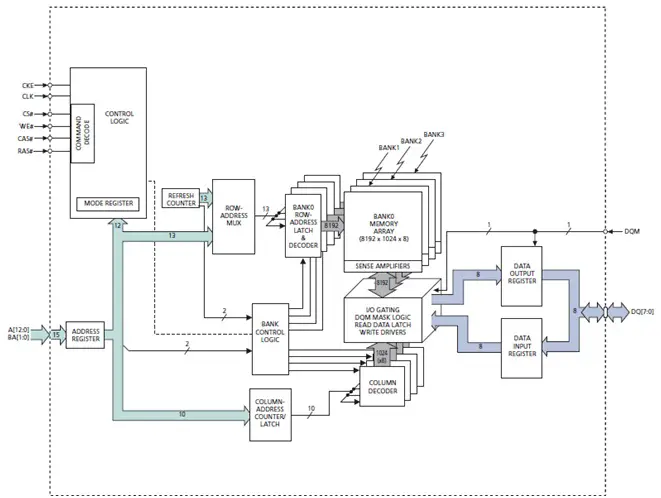
Memory calculations for above memory SDR SDRAM organizations:-
Data Bus Width = 8-Bits
No of Row Address Bits: – 13
No of Column Address Bits: – 10
No of Banks = 4
Total number of Memory locations in the SDR SDRAM=
2^No of Row Address Bits x 2^ No of Column Address Bits x No of Banks
= 2^13 x 2^ 10 x 4 = 2^13 x 2^ 10 x 2^2 = 2^25 = 32 Mega locations
Total Size of SDR SDRAM memory =
Data Bus Width x Total number of Memory locations in the SDR SDRAM
= 8-Bits x 32 Mega locations = 256 Mega Bits
16 Meg x 16 Functional Block Diagram
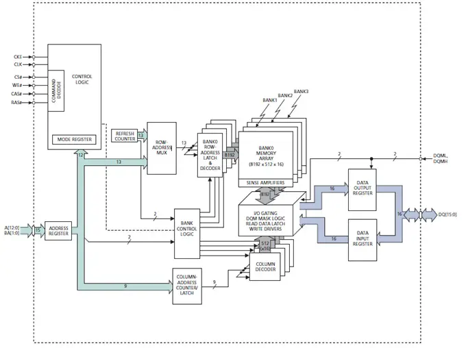
Memory calculations for above memory SDR SDRAM organizations:-
Data Bus Width = 16-Bits
No of Row Address Bits: – 13
No of Column Address Bits: – 9
No of Banks = 4
Total number of Memory locations in the SDR SDRAM=
2^No of Row Address Bits x 2^ No of Column Address Bits x No of Banks
= 2^13 x 2^ 9 x 4 = 2^13 x 2^9 x 2^2 = 2^24 = 16 Mega locations
Total Size of SDR SDRAM memory =
Data Bus Width x Total number of Memory locations in the SDR SDRAM
= 16-Bits x 16 Mega locations = 256 Mega Bits
SDRAM Commands
SDRAM (Synchronous Dynamic Random-Access Memory) commands and their meanings are provided as below. These commands are essential for controlling the operation and data access of SDRAM devices. Here’s a summary of these commands and their functions:
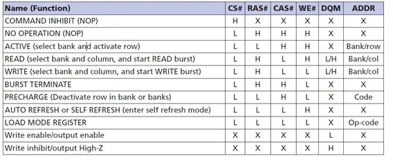
ACTIV (Bank Activate Command):
- Activates a specific bank in the SDRAM.
- Row addresses are latched on address pins (A0 to A10).
- Another command cannot be issued until the Row-to-Column Delay (RCD) has been met.
- Used to open a row for read or write operations.
PRCG (Precharge All Command):
- Precharges both banks simultaneously.
- Transitions the SDRAM to the idle state.
- A further command cannot be issued until the Precharge time (tRP) has been met.
- Precharging is necessary to close a row after read or write operations.
WRITE (Write Command):
- Performs a write access to the bank selected by the Bank Select (BS) signal.
- Data is latched on the positive edge of the system clock (CLK).
- The burst length and addressing mode are configured in the Mode Register at power-up.
- Data is written to the opened row in the selected bank.
WRITEA (Write with Auto-precharge Command):
- Similar to the WRITE command but automatically performs a precharge operation after the write.
- This command cannot be interrupted by other commands.
- A further command cannot be issued until the Precharge time (tRP) has been met.
READ (Read Command):
- Performs a read access to the bank selected by Bank Select (BS).
- Data is issued on the positive edge of the clock (CLK) at a time defined by the CAS latency (ICAS).
- Reads data from the opened row in the selected bank.
READA (Read with Auto-precharge Command):
- Similar to the READ command but automatically performs a precharge operation after the read.
- This command cannot be interrupted by other commands.
- A further command cannot be issued until the Precharge time (tRP) has been met.
MRS (Mode Register Set Command):
- Programs the CAS latency, addressing mode, and burst length in the mode register.
- This command must be configured after power-up because the mode register is undefined after a reset.
- A further command cannot be issued until the Register Set Cycle (RSC) is met.
NOP (No-Operation):
- Performs no operation; it is equivalent to deselecting the device.
- Used when no other operation is required, and it doesn’t affect the device’s state.
REF (Auto-refresh Command):
- Used to refresh the SDRAM by accessing a specific row address provided by the internal refresh counter.
- Equivalent to a CAS (Column Address Strobe) before RAS (Row Address Strobe) refresh in conventional DRAM.
SDR SDRAM Controller is a Hardware Component
The SDR SDRAM Controller is a hardware component designed to manage and control Single Data Rate Synchronous Dynamic Random Access Memory (SDR SDRAM) operations. It is divided into four main modules:
- SDRAM Controller Module: This is the top-level module responsible for coordinating and overseeing the entire SDR SDRAM control process, it instantiates the other three lower modules and integrates them into a cohesive system. The SDRAM Controller Module manages the timing and sequencing of commands and data transfers to and from the SDRAM
- Control Interface Module: The Control Interface Module serves as the interface between the host (often a processor or memory controller) and the SDR SDRAM Controller. It receives commands and related memory addresses from the host, decodes these commands, and then passes the appropriate requests to the Command Module for execution. This module essentially translates high-level commands from the host into the low-level commands required by the SDRAM
- Command Module: The Command Module is responsible for receiving the commands and addresses from the Control Interface Module. It interprets these commands and generates the necessary control signals and commands to be sent to the SDRAM device. The Command Module ensures that the SDR SDRAM operates according to the host’s instruction
- Data Path Module: The Data Path Module handles data operations during WRITEA (write access) and READA (read access) commands. It manages the transfer of data between the host and the SDRAMA. This module ensures that data is correctly written to or read from the memory and that it follows the appropriate data path
- Additionally, a PLL (Phase-Locked Loop) in the SDR SDRAM Controller, PLL is used in CLOCK LOCK mode to improve I/O (Input/Output) timing, PLLs are used for dock synchronization and can help manage clock skew and jitter in the system. While the PLL is not essential for the basic operation of the SDR SDRAM Controller, it can be beneficial for ensuring the correct timing of signals in the system
Summary
Here’s the information summarized in bullet points:
SDR SDRAM (Single Data Rate Synchronous Dynamic Random-Access Memory):
- Early type of SDRAM technology.
- Transfers data on the rising edge of the clock signal (Single Data Rate).
- One data transfer per clock cycle.
- Lower data transfer rate compared to later SDRAM types like DDR SDRAM.
- Outdated and replaced by more advanced DDR SDRAM technologies.
Key Specifications of SDR SDRAM Memory:
- Typical operating voltage: 3.3V
- Prefetch architecture: 1N
- Input/output logic level: LVTTL-compatible
- CAS latency: 2-3 clock cycles
- Clock speeds: 66 MHz, 100 MHz, 132 MHz, 166 MHz
- Data rate: 100/133/166 Mbps
- Clock input: Single clock (rising edge)
- Burst length: 1, 2, 4, 8, or full page
- Data strobe: Unsupported
SDR SDRAM Addressing:
- Row and column addresses used to access data within the module.
- Row address selects the row, and column address selects the column.
- Bank address may also be used in multi-bank SDRAM devices.
- Memory rank specifies the rank of memory modules in multi-rank configurations.
SDR SDRAM Controller:
- Hardware component managing SDR SDRAM operations.
- Comprises four modules: SDRAM Controller, Control Interface, Command, and Data Path.
- Synchronizes and executes memory commands and data transfers between the host and SDR SDRAM.
Author Profile
- 20+ years embedded hardware design professional with a burning passion for teaching. Sharing the intricate world of embedded hardware is my mission and joy.
Latest entries
 Tech Updates30 November 2025STM32WBA6: The Next-Generation MCU Powering Secure Short-Range Wireless Designs
 Blogs24 November 2025High-Speed PCB Layout Design Guide-104
 Tech Updates14 September 2025Renesas Launches RL78/L23 Ultra-Low-Power MCUs to Power Smarter Home Appliances
 Blogs7 September 2025High-Speed PCB Layout Design Guide-103