Flash memory is an electrically erasable programmable ROM memory that allows block/sector erase and re-programming. It offers faster erase and write times. Flash memory is widely used in embedded systems due to its non-volatile nature, higher density, and faster access times.
It is commonly utilized for firmware storage, system booting, and data storage in a wide range of embedded devices. The most common types of flash memories are NOR Flash, NAND Flash, and eMMC Flash.
Selecting the appropriate Flash memory for an embedded system is indeed a critical decision for designers. Both NOR Flash Memory and NAND Flash Memory have distinct characteristics that make them suitable for different applications.
We will touch upon the following topics as a part of this blog:
What is NOR Flash?
NOR flash is a type of non-volatile memory used for storing data in electronic devices. Key characteristics of NOR flash include random access, allowing individual memory cells to be directly addressed, execute-in-place (XIP) capability for executing code directly from the memory itself, high endurance (number of erase/write cycles), and higher cost per gigabyte compared to NAND flash.
These characteristics make NOR Flash Memory particularly well-suited for applications where random access and XIP are essential, such as embedded systems, and certain consumer electronics products.
Additionally, its high endurance makes it suitable for applications requiring frequent updates, like firmware storage or boot code.
However, due to its cost, it is more commonly used in smaller memory requirements and specialized applications where its unique features are advantageous.
What are the characteristics and features of NOR Flash Memory?
- Random Access: NOR flash Memory allows individual memory cells to be directly addressed, which means data can be read and written at random, similar to the operation of traditional RAM (Random Access Memory).
- Execute-in-Place (XIP): One of the main advantages of NOR flash memory is its ability to execute code directly from the memory itself. By executing code directly from NOR flash, embedded systems can save RAM for other tasks and streamline the boot process. It is especially advantageous for applications that require fast boot times, such as in automotive systems, routers, industrial controllers, and other embedded devices. This makes it more suitable for applications where data is read more frequently than written, like firmware storage or boot code.
- High Endurance: NOR flash Memory has a higher endurance (number of erase/write cycles), making it more suitable for applications that require frequent updates.
- Expensive: NOR Flash Memory tends to be more expensive on a per-gigabyte basis compared to NAND flash. As a result, it is often used for firmware storage or boot code.
The Architecture of NOR Flash Memory
Flash memory stores information in an array of memory cells, and the data is stored by trapping electric charges in floating-gate transistors.
Flash memory cells are based on floating-gate transistors. Each cell has a floating gate, which is a conductive or non-conductive layer that is electrically isolated by an insulating layer.
The charge on the floating gate determines the state of the memory cell, representing either a “0” or a “1” bit.
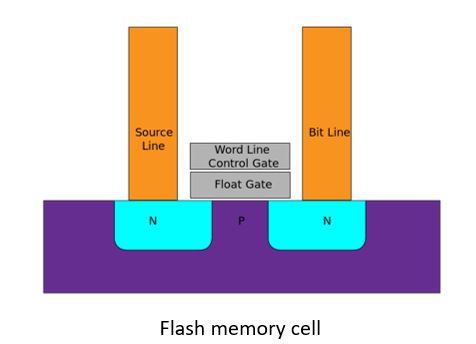
NOR Flash memory has a parallel access architecture, which means that each memory address can be directly accessed without having to go through the entire memory sequentially.
This characteristic makes NOR flash memory suitable for applications that require executing code directly from memory, such as in microcontrollers and BIOS chips.
![]()
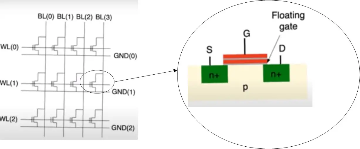
The NOR Flash memory array consists of double-gate transistors arranged in rows and columns, similar to a regular NOR array. It has ground lines, word lines derived from row decoders, bit lines connected to column decoders, and sense amplifiers for reading data.
NOR Flash Memory Programming
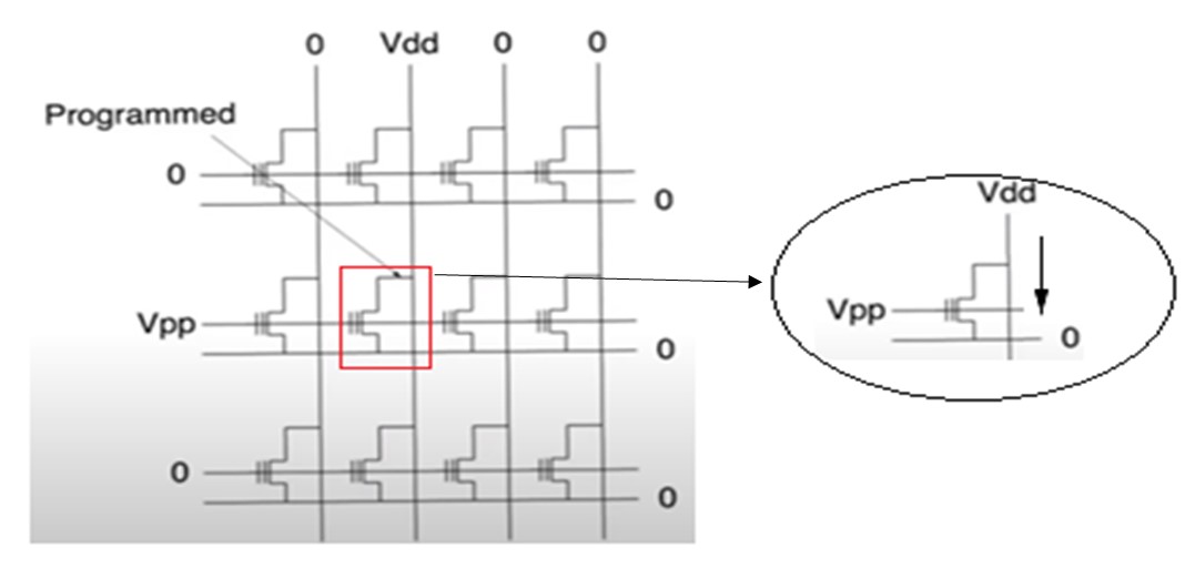
To program a specific cell, a high voltage (VPP) is applied to the gate (word line) of the target cell, creating a high-speed electron flow in the channel.
This process, known as hot carrier injection, enables a large number of electrons to be attracted into the floating gate, changing the cell’s state.
During programming, adjacent cells in the same row (Row 2) may also experience light tunneling due to the VPP applied to their gates. However, since programming via hot carrier injection is relatively fast than tunneling, the effect on these adjacent cells is negligible, and their values remain unchanged.
Monitoring and Control of NOR Flash Memory Cells
Flash memory cells are sensitive to various factors that can affect their performance and reliability over time. One critical parameter that requires monitoring is the threshold voltage, which determines the state of each memory cell (e.g., whether it is programmed or erased).
Variations in threshold voltage can occur due to factors like program/erase cycles and environmental conditions. To maintain data integrity and extend the lifespan of the Flash memory, control circuits are necessary to monitor and adjust these threshold voltage values.
NOR Flash Memory Erasing
As shown in the below picture, to erase a cell, a voltage applied is a VPP on the source, a “0V” on the control gate, and an open circuit on the drain is applied. As the cell is programmed it has an electron on the floating gate. To erase the call, these electrons have to tunnel back to the substrate.
When below voltages are applied, it creates a large vertical field that promotes the flow of electrons back into the substrate, effectively erasing the cell. However, this erasing process affects the entire row, and adjacent cells may also experience tunneling, leading to undesired changes in their values.
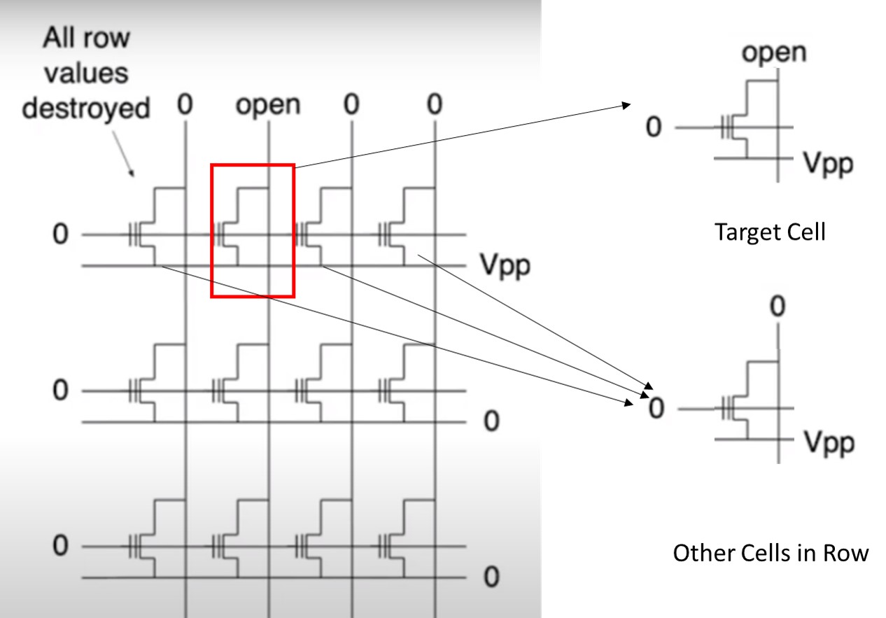
Unlike programming, erasing a specific cell in a NOR Flash memory array is not practical. If you want to erase only one cell in a row, you’d have to read the contents of the entire row, save them into registers, erase the row, and then rewrite everything except the cell you wanted to erase. This process is cumbersome and may require additional circuitry to manage.
In summary, NOR flash memory can be erased on a block-wise basis, resetting all cells within the block to the “1” state using high-voltage pulses.
Programming, on the other hand, can be done at a more granular level, allowing data to be written one byte or word at a time, providing versatility for data updates without erasing the entire block.
Type of NOR Flash Memory
- Single-Level Cell (SLC): In SLC flash devices, each NOR Flash Memory cell stores only one bit of information. The floating gate in an SLC cell can be in one of two distinct charge states, representing “0” or “1.” This simplicity allows for faster read and write operations and higher endurance compared to Multi-Level Cell (MLC) flash.
- Multi-Level Cell (MLC): MLC NOR Flash Memory devices can store more than one bit per cell. By partitioning the floating gate into multiple charge states, MLC cells can represent two or more bits of data. Common MLC configurations include two bits per cell (2-bit MLC) and three bits per cell (3-bit MLC or TLC). MLC offers higher data storage density but may have slightly slower read and write speeds compared to SLC.
- SONOS Flash Memory: SONOS (Silicon-Oxide-Nitride-Oxide-Silicon) NOR Flash Memory is a type of non-volatile memory that uses a non-conductive material (typically nitride) as the charge-trapping layer in the floating-gate transistor. SONOS flash is known for its reliability and scalability, making it a popular choice in certain applications.
Each type of NOR Flash Memory, SLC, MLC, and SONOS—has its own advantages and is chosen based on the specific requirements of the application, balancing factors such as performance, endurance, and cost.
NOR Flash Advantages
- Sufficient Address mapping capability: NOR Flash Memory provides enough address lines to map the entire memory range, enabling random access and short read times.
- Ideal for Code Execution: The random access capability makes it suitable for executing code directly from memory, making it useful in microcontrollers, BIOS chips, and other applications where fast code execution is crucial.
- Known Good Bits: NOR Flash Memory offers 100% known good bits for the entire lifespan of the part, enhancing its reliability.
- Reliability: NOR Flash Memory has a lower susceptibility to bit-flipping, making it more reliable in preserving stored data. It is shipped with zero bad blocks and has a lower bad block accumulation during its lifespan.
NOR Flash Disadvantages
- Larger Cell Size: NOR Flash Memory has a larger cell size, resulting in a higher cost per bit compared to NAND Flash.
- Slower Write and Erase Speeds: NOR Flash Memory exhibits slower write and erase speeds compared to NAND Flash.
Point to Remember
- NOR Flash Memory is a type of non-volatile memory used for storing data in electronic devices.
- NOR Flash Memory cells have one end connected directly to the ground and the other end connected to a bit line, resembling a NOR gate in digital logic.
- NOR Flash Memory offers random access, allowing individual memory cells to be directly addressed, similar to traditional RAM.
- It supports execute-in-place (XIP) capability, enabling code to be executed directly from the memory, making it suitable for microcontrollers and embedded systems.
- NOR Flash Memory has a higher endurance (number of erase/write cycles) compared to NAND flash, making it suitable for applications that require frequent updates.
- NOR Flash Memory tends to be more expensive on a per-gigabyte basis compared to NAND flash.
- NOR Flash Memory is commonly used for firmware storage, system booting, and data storage in various devices.
- It has known good bits for the entire lifespan, enhancing its reliability.
- NOR Flash Memory has slower write and erase speeds compared to NAND flash, but it is more suitable for applications where data is read more frequently than written.
Author Profile
- 20+ years embedded hardware design professional with a burning passion for teaching. Sharing the intricate world of embedded hardware is my mission and joy.
Latest entries
 Tech Updates30 November 2025STM32WBA6: The Next-Generation MCU Powering Secure Short-Range Wireless Designs
 Blogs24 November 2025High-Speed PCB Layout Design Guide-104
 Tech Updates14 September 2025Renesas Launches RL78/L23 Ultra-Low-Power MCUs to Power Smarter Home Appliances
 Blogs7 September 2025High-Speed PCB Layout Design Guide-103

