DDR SDRAM (double data rate synchronous DRAM) is a type of SDRAM that realizes twice the data transfer rate of conventional SDR SDRAM. In SDR SDRAM, data is transferred on the rising edge of the clock signal. On the other hand, DDR SDRAM transfers data on both the rising and falling edges of the clock signal, effectively doubling the data transfer rate compared to SDR SDRAM.
This double data rate enables DDR SDRAM to achieve higher bandwidth and improved performance, making it a more efficient choice for memory-intensive tasks. Additionally, DDR SDRAM tends to operate at lower power consumption compared to its predecessor.
It’s worth noting that there are different generations of DDR SDRAM, such as DDR2, DDR3, DDR4, and DDR5, each introducing further improvements in terms of speed, efficiency, and capacity. These advancements have contributed to the overall performance improvements in computer systems over the years.
Specification of DDR Vs SDR SDRAM Memory
|
Parameters |
DDR SDRAM |
SDR SDRAM |
|
Typical Operating Voltage |
2.5V, 1.8V(Low Voltage) |
3.3V |
|
Prefetch Architecture |
2N |
1N |
|
Data Transfer Rate |
2/tck (Clock cycle time) |
1/tck (Clock cycle time) |
|
input/output logic level |
SSTL_2-compatible |
LVTTL-compatible |
|
/CAS read latency |
2-2.5 Clock cycle |
2-3 Clock cycle |
|
/CAS write latency |
1 Clock cycle |
0 Clock cycle |
|
Clock Speed(Internal) |
100 MHz, 133 MHz, 166 MHz, 200 MHz |
66 MHz, 100 MHz, 133 MHz |
|
Data Rate |
200- 400 Mbps |
66 – 133 Mbps |
|
Clock input |
Differential Clock (Rising & Falling edge) |
Single Clock (Rising edge) |
|
Burst Length |
2, 4, 8 |
1, 2, 4, 8, full page |
|
Data Strobe |
Essential |
Unsupported |
Functionality of DDR VS. SDR SDRAM
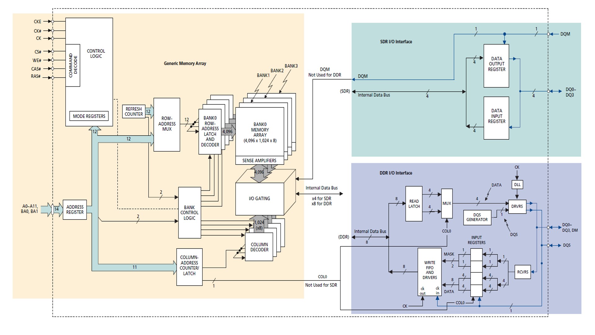
The comparison of the functional block diagrams for the 32 Meg x 4 Single Data Rate (SDR) and Double Data Rate (DDR) memory indicates a fundamental similarity in the memory core structure, as illustrated in above Figure. Despite potential differences in their operational aspects, the core components and organization of the memory appear to align closely between SDR and DDR configurations.
While both share an identical addressing and command control interface, a four-bank memory array, and common refresh requirements, the key differences lie in the data handling mechanisms. SDR employs a fully synchronous design, capturing data only on the positive clock edge, with an internal bus matching the external data bus width.
DDR, on the other hand, adopts a true source-synchronous design, capturing data twice per clock cycle with a bidirectional data strobe. DDR features a 2n-prefetch architecture, allowing the internal memory cell to pass data more efficiently, and supports a BURST TERMINATE command for quick READ termination. Notably, DDR lacks an output enable for READ operations but introduces the DM signal during WRITE operations to mask nonvalid write data.
New Features of DDR SDRAM
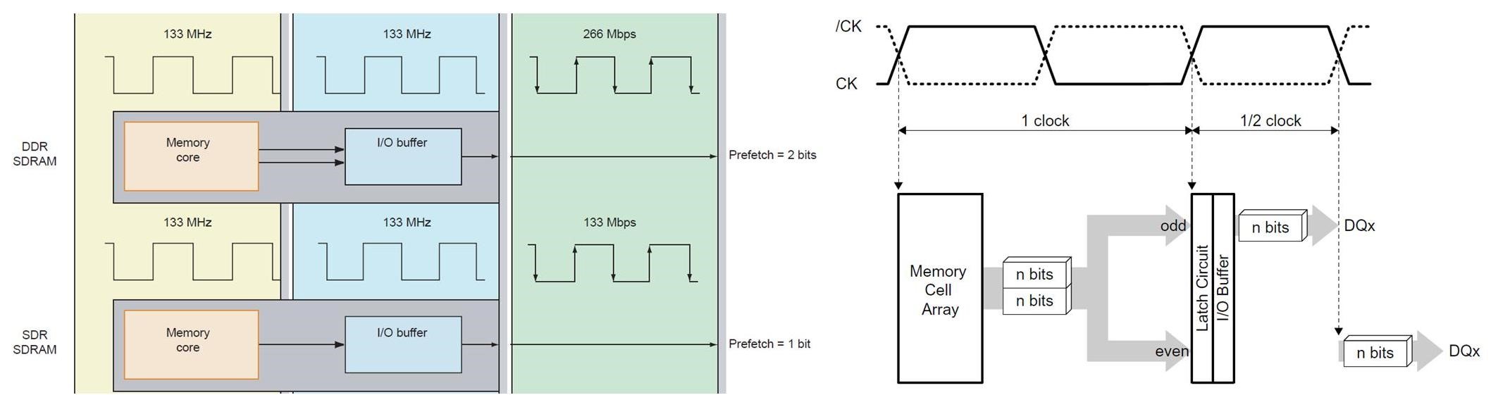
Concept of 2n-Prefetch
DDR SDRAM (Double Data Rate Synchronous Dynamic Random Access Memory) achieves a data transfer rate twice the clock frequency through the use of a 2-bit prefetch architecture. Through its 2-bit prefetch architecture, DDR SDRAM (Double Data Rate Synchronous Dynamic Random Access Memory) achieves a data transfer rate twice the clock frequency.
This design involves transferring 2n bits of data from the memory cell array to the I/O buffer during each clock cycle. The data is then output n bits at a time on both the rising and falling edges of the clock, occurring every half clock cycle.
Key to this architecture is the internal bus width being twice that of the external bus width, allowing for the concurrent transfer of multiple bits and enhancing data output rates. As a result, DDR SDRAM supports burst lengths of 2, 4, and 8. This means that data access and transfer operations are optimized, with consecutive data words fetched in pairs.
In below picture we can see that SDR SDRAM, where 1-Bit Prefetch Architecture with internal memory cell and I/O buffer running with speed of 133MHz. As data is sampled at rising edge of clock, I/O buffer can transfer the data with speed of 133Mbps. On the other hand DDR SDRAM, where 2-Bit Prefetch Architecture memory cell is ready with 2 bit data and same can be sampled at both rising and falling edge of clock achieving the data rate of 266Mbps.
Clock Input(CK, nCK)
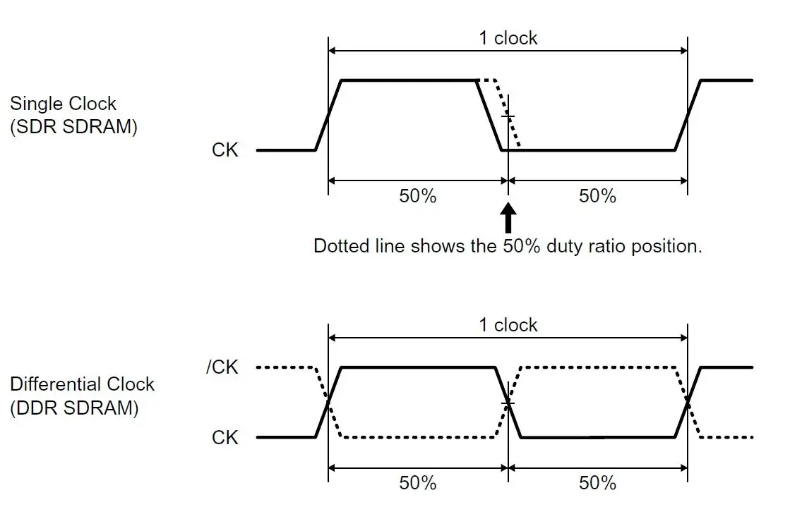
In Single Data Rate Synchronous Dynamic Random-Access Memory (SDR SDRAM), where data input/output is synchronized only with the rising edges of the clock, there is typically some margin in the timing. However in the case of Double Data Rate Synchronous Dynamic Random-Access Memory (DDR SDRAM), where data input/output is synchronized with both the rising and falling edges of the clock, controlling the timing accurately becomes more challenging when relying on a conventional single clock.
To address this challenge, DDR SDRAM adopts a differential clock scheme. A differential clock involves two signals that are the inverse of each other (one rising when the other is falling). This differential clocking mechanism helps in achieving more precise control over the data input and output timing.
By using both the rising and falling edges of the clock, DDR SDRAM can effectively double the data transfer rate compared to SDR SDRAM. The differential clocking scheme is a key innovation that enables the increased efficiency and performance of DDR SDRAM.
Due to factors such as variations in clock distribution networks, fluctuations in the clock source, diverse load conditions, and other influences, the duty cycle of the clock input in DDR SDRAM may deviate from the ideal 50%, where the high-level period and low-level period are not equal.
In DDR SDRAM, the synchronization of data input/output occurs with both the rising and falling edges of the data strobe signal (DQS), mirroring the period of the clock input (CK). The utilization of a differential clock scheme plays a crucial role in enabling DDR SDRAM to accommodate higher clock frequencies while concurrently mitigating the adverse effects of noise and other influencing factors.
Data Strobe Signal (DQS)
DDR SDRAM, Similarly to SDR SDRAM, is controlled by command input signals synchronized with the rising edge of the clock (CK). However, its data input/output timing differs, as DDR SDRAM transfers data on both the rising and falling edges of the clock signal, effectively doubling the data transfer rate compared to SDR SDRAM.
To achieve high-speed data transfer, DDR SDRAM introduces a data strobe signal called DQS, which is output from memory controller to DDR SDRAM. This DQS signal is essential for adjusting the data capture timing at the receiver end, ensuring accurate sampling of data (DQ) even at higher clock speeds.
The receiver utilizes the DQS signal to fine-tune the timing for capturing the data, thereby enhancing data integrity and reliability in the process. In summary, DDR SDRAM employs a combination of dual-edge data transfer and the use of a data strobe signal (DQS) to achieve faster data transfer rates while maintaining precise data capture timing.
Interface Voltage Logic
DDR SDRAM employs the SSTL_2 (Stub Series Terminated Logic for 2.5V) interface, a low-voltage (2.5V), small-amplitude, high-speed design. This interface reduces signal degradation caused by noise and reflections at high frequencies by incorporating series resistors between the signal branch point and the memory, enhancing overall signal integrity.
- Stub Resistance: Around 25Ω (22Ω for DIMMs) stub resistance connects to the output pin (VOUT) for impedance matching, aligning the transmission line with the device output.
- Termination Voltage: VTT line is terminated with approximately 25Ω (27Ω for DIMMs), reducing signal reflection and voltage spikes, facilitating high-speed data transmission.
- Reference Voltage: SSTL_2 interface, symmetrical for high and low levels, uses VREF as a reference voltage for level detection.
- Interface Specification: DDR SDRAM typically employs SSTL_2 with termination at one end for signal integrity.
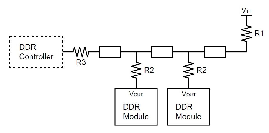
R1: Termination resistance (27W)
R2: Stub resistance (22W) (Mounted on DIMM)
R3: (22W)
VTT = 1/2 VDDQ
Operating Voltage
Transition from Single Data Rate (SDR) SDRAM, which typically operates on a 3.3V power supply, to Double Data Rate (DDR) SDRAM with a lower 2.5V power supply represents a reduction in power supply voltage. This decrease in voltage in DDR SDRAM circuits contributes to a reduction in power consumption.
Lowering the power supply voltage is a common strategy to enhance energy efficiency and reduce heat generation in electronic components. It aligns with efforts to design more power-efficient and performance-oriented memory technologies.
Delay Locked Loop (DLL)
DDR SDRAM (Double Data Rate Synchronous Dynamic Random Access Memory) is equipped with a Delay Locked Loop (DLL) circuit. The purpose of this DLL circuit is to achieve a fast access time and support high operating frequencies. It achieves this by controlling and adjusting the time lag between the external clock and the internal clock signals.
The DLL helps in synchronizing these clocks effectively, ensuring proper timing for data transfers and enabling the memory to operate efficiently at high frequencies. This synchronization is crucial for the overall performance and reliability of DDR SDRAM in modern computing systems.
DDR SDRAM Commands
In DDR SDRAM (Double Data Rate Synchronous Dynamic Random Access Memory), the memory controller communicates with the memory module by issuing commands at the rising edge of the clock signal (CK). The rising edge of the clock signal is used as a reference point for the timing of commands and data transfers.
This synchronous operation ensures that data is transferred and commands are executed in a coordinated manner, enhancing the overall efficiency and reliability of the memory system.
DDR SDRAM (Synchronous Dynamic Random-Access Memory) commands and their meanings are provided as below. These commands are essential for controlling the operation and data access of DDR SDRAM devices. Here’s a summary of these commands and their functions:
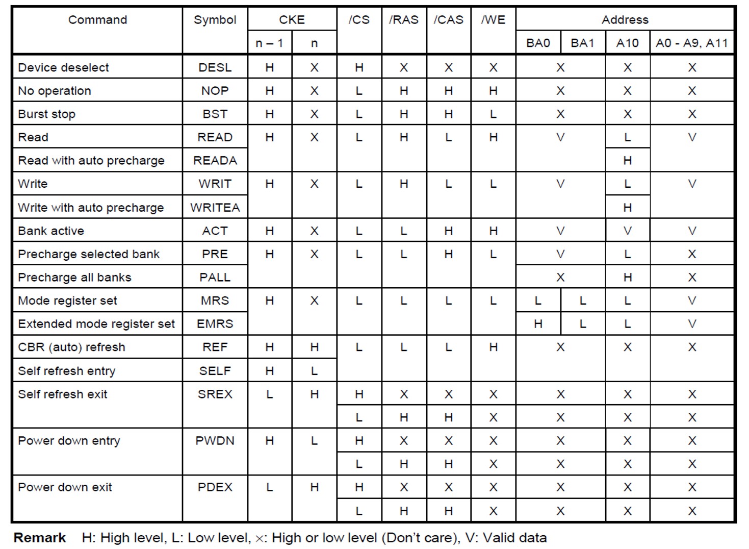
The DDR SDRAM operates through a series of defined command states, each serving a specific function in the memory access process:
- Idle (IDLE): The bank is precharged, and tRP (precharge time) has been satisfied. Only certain commands (ACT, MRS, EMRS, REF, SELF) can be issued when the device or selected bank is in the idle state.
- Bank Activating (Row Activating): Before performing a read or write operation for a specific row in a bank, the bank must be activated. This state is entered when the ACT command is issued, and it transitions to the bank active state when tRCD (row-to-column delay) is satisfied.
- Bank Active (BANK ACTIVE) (Row Active): The device is ready to receive a read or write command when tRCD is satisfied, signifying that the bank is active.
- Precharge: After completing a read or write operation, the bank must return to the idle state to activate a different row. The PRE (precharge) command is issued, and the state transitions to precharge until tRP is satisfied, at which point the bank returns to the idle state.
- Read and Write (READ, WRIT): The state during an active read or write operation. The read or write command, along with a column address for the active bank, initiates the operation. After completion, the bank automatically returns to the bank active state.
- Read and Write with Auto Precharge (READA, WRITA): Initiates a read or write operation with automatic precharge. The bank automatically starts precharging, and after completing the read or write operation, it returns to the idle state.
- Mode Register Set: The mode register set or extended mode register set command (MRS, EMRS) can only be issued when all banks are in the idle state. After writing data to the mode register, the device automatically returns to the idle state after tMRD.
- CBR (Auto) Refresh: The CBR (auto) refresh command (REF) can only be issued when all banks are in the idle state. It selects a row address in every bank for refresh, and after CBR (auto) refresh is completed, the device returns to the idle state after tRFC (refresh cycle time). These commands are crucial for maintaining the integrity and efficiency of DDR SDRAM operation.
Summary
- DDR SDRAM Overview:
- DDR SDRAM (Double Data Rate Synchronous Dynamic Random Access Memory) achieves twice the data transfer rate of SDR SDRAM by transferring data on both rising and falling edges of the clock signal.
- Different generations of DDR SDRAM (DDR2, DDR3, DDR4, DDR5) have been developed, introducing improvements in speed, efficiency, and capacity.
- Specifications and Comparison with SDR SDRAM:
- DDR SDRAM operates at lower voltages (2.5V, 1.8V) compared to SDR SDRAM (3.3V).
- DDR uses a 2N prefetch architecture, achieving a data transfer rate of 2/tck, while SDR has a 1N prefetch architecture with a data transfer rate of 1/tck.
- DDR employs SSTL_2-compatible input/output logic, while SDR uses LVTTL-compatible logic.
- Latencies, clock speeds, and data rates differ between DDR and SDR SDRAM.
- Functional Block Diagram Comparison:
- Functional block diagrams for 32 Meg x 4 SDR and DDR SDRAM show similarities in core structure, but differences in data handling mechanisms.
- DDR employs a true source-synchronous design with a 2N prefetch architecture, supporting burst lengths of 2, 4, and 8.
- New Features of DDR SDRAM:
- DDR SDRAM introduces a 2-bit prefetch architecture, achieving a data transfer rate twice the clock frequency.
- The differential clock scheme ensures precise control over data input/output timing.
- The data strobe signal (DQS) is introduced to adjust data capture timing, enhancing data integrity.
- Interface Voltage Logic:
- DDR SDRAM uses the SSTL_2 interface, a low-voltage (2.5V) design with series resistors for signal integrity.
- Stub resistance, termination voltage (VTT), and reference voltage (VREF) are key components of the interface.
- Delay Locked Loop (DLL):
- DDR SDRAM incorporates a DLL circuit to synchronize external and internal clock signals, ensuring fast access times and supporting high operating frequencies.
- DDR SDRAM Commands:
- DDR SDRAM operates through various command states, including Idle, Bank Activating, Bank Active, Precharge, Read/Write, Read/Write with Auto Precharge, Mode Register Set, and CBR (Auto) Refresh.
- Commands are issued at the rising edge of the clock signal, and each state serves a specific function in the memory access process.
In summary, DDR SDRAM stands out with its dual-edge data transfer, 2-bit prefetch architecture, and advanced features like the data strobe signal (DQS) and differential clocking. These attributes contribute to its higher performance, efficiency, and reliability in comparison to SDR SDRAM.
Author Profile
- 20+ years embedded hardware design professional with a burning passion for teaching. Sharing the intricate world of embedded hardware is my mission and joy.
Latest entries
 Tech Updates30 November 2025STM32WBA6: The Next-Generation MCU Powering Secure Short-Range Wireless Designs
 Blogs24 November 2025High-Speed PCB Layout Design Guide-104
 Tech Updates14 September 2025Renesas Launches RL78/L23 Ultra-Low-Power MCUs to Power Smarter Home Appliances
 Blogs7 September 2025High-Speed PCB Layout Design Guide-103