SDRAM stands for Synchronous Dynamic Random-Access Memory, which is a type of dynamic random-access memory (DRAM) that operates in synchronization with the System/CPU clock of the memory controller (SDRAM Controller of Microprocessor). This synchronization is a fundamental characteristic of SDRAM and sets it apart from asynchronous DRAM technologies.
The synchronization with the system clock enables precise and predictable memory access, making SDRAM faster and more efficient than earlier asynchronous DRAM types. It ensures that data transfers and memory commands occur at specific points in the clock cycle, allowing for optimal memory performance in modern computer systems.
SDRAM is widely used as the primary system memory (RAM) in various computing devices, including desktops, laptops, servers, embedded systems, and many other electronic devices where fast and synchronized memory access is essential for smooth operation and performance.
We will touch upon the following topics as a part of this blog.
Importance of SDRAM in Computer Memory Hierarchy
SDRAM occupies a critical position within the computer memory hierarchy. In this hierarchy, it sits between the CPU’s high-speed cache memory and slower, non-volatile storage mediums like hard drives or solid-state drives (SSDs).
Its significance lies in its role as the primary working memory (RAM) of a computer. When a program runs, the CPU actively accesses and manipulates data stored in SDRAM.
Also read: How to interface SDR SDRAM Memory?
This rapid and direct data access significantly accelerates system performance compared to retrieving data from slower secondary storage devices. As a result, SDRAM plays a crucial role in enabling computers to run applications smoothly and responsively.
The Architecture of SDRAM Memory
The architecture of SDRAM (Synchronous Dynamic Random-Access Memory) determines how data is stored, accessed, and managed within the memory module.
SDRAM memory is organized into an array of memory cells. Each memory cell typically consists of a cell capacitor (Storage Node) in series with an access nMOS transistor (as shown in the below picture), each capable of storing one bit of data.
This array of memory cells is organized into rows and columns. Rows are often referred to as word lines, while columns are known as bit lines. Rows and columns intersect at specific memory cell locations, allowing for the selection of individual cells as seen in the below picture. Further SDRAM memory is divided into multiple banks, each containing an equal portion of the total memory sizes.
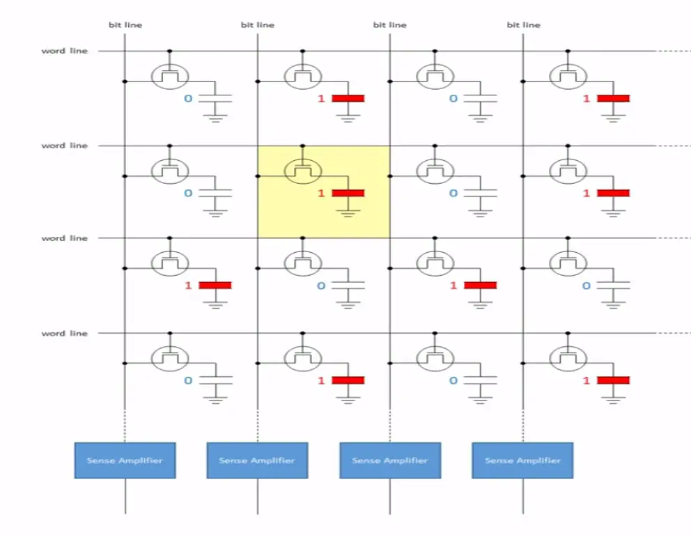 SDRAM-Memory-Cell-Array
How to access SDRAM Memory?
Memory stores binary data by utilizing a capacitor (the presence or absence of electrical charge). A binary bit value is stored on this capacitor, with a charged capacitor representing a “1” and a discharged capacitor representing a “0.”
This storage mechanism is facilitated by an nMOS (n-channel Metal-Oxide-Semiconductor) transistor, which functions as a switch within the bit cell, connecting or disconnecting the capacitor from the bit line.
The nMOS opens and closes based on the voltage on the wordline, charging or draining the capacitor attached to it. When the word line is asserted, the nMOS transistor turns ON, allowing the transfer of charge to or from the storage capacitor to the bitline, thereby altering the charge level on the capacitor to reflect the stored data value.
To access a specific memory location, the memory controller sends a bank address, a row address, and a column address. As per the bank address appropriate bank is selected. The row address selects the appropriate row (wordline), activating it for reading or writing.
The column address selects the specific memory cell within the activated row. The nMOS transistor either connects or disconnects the storage capacitor from the bit line. When a read operation is initiated, the sense amplifiers are activated.
They compare the charge in the selected memory cells to a reference voltage. Depending on whether the charge is higher or lower than the reference voltage, the sense amplifiers produce an output that corresponds to logic 0 or logic 1.
The presence or absence of charge on the storage capacitor is sensed and amplified, which further represents the binary data value “1,”(Charged) and a binary “0.”(Discharged)
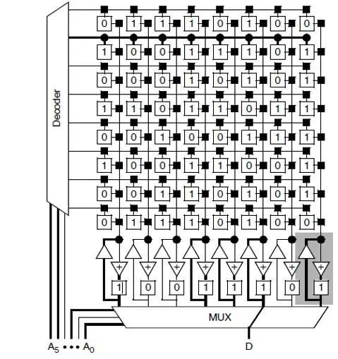
The figure shows an SDRAM array with 8 row and column lines which form a 64-bit array. Remember, the row count is always greater than or equal to the column count due to a variety of design reasons.
This array holds 64 bits but can only read or write 1 bit of information at a time. For this reason, SDRAM has further segmentations in its architecture. An 8-bit port size SDRAM has 8 arrays, each the same size. When access is requested, the memory only requires 1 address to access 1 bit from each of the 8 arrays to provide 8 bits of data.
Features of SDRAM
Synchronous Operation of SDRAM Memory
Synchronous operation is a fundamental characteristic of SDRAM that sets it apart from earlier memory technologies like DRAM. SDRAM synchronizes its data transfer and memory access with the system clock, ensuring that data is read from or written to the memory at precise and predictable intervals.
This synchronization allows for efficient coordination between the CPU and memory, as both operate in harmony with the same clock signal.
As a result, SDRAM can precisely time its operations, reducing latency and maximizing data throughput. This synchronous nature makes it well-suited for high-speed and real-time applications, where timing accuracy is crucial.
SDRAM Memory Refresh/Auto-Refresh
Over time, due to inherent electrical characteristics and materials used, the charge stored in these capacitors can gradually leak away. This is a natural process and occurs even if the memory is not being actively used.
To prevent the loss of data, SDRAM cells need to be periodically refreshed, typically every few milliseconds. During a refresh operation, the memory controller reads and then immediately rewrites the data back into the same cells.
This process restores the charge in the capacitors to their original state, effectively “refreshing” the data. SDRAM has specific command and timing sequences for refreshing the memory. The “refresh command” in SDRAM is part of its protocol and is used to initiate the refresh operation.
“AUTO REFRESH” command is used during normal operation of the SDRAM. The SELF REFRESH command can be used to retain data in the SDRAM, even if the rest of the system is powered-down. When in the self-refresh mode, the SDRAM retains data without external clocking
For example regardless of device width, the 256Mb SDRAM requires 8192 AUTO REFRESH cycles every 64ms (commercial and industrial) or 16ms (automotive). Providing a distributed AUTO REFRESH command every 7.813μs (commercial and industrial) or 1.953μs (automotive) will meet the refresh requirement and ensure that each row is refreshed.
SDRAM Memory Precharge/Auto-Precharge
SDRAM cells are organized into banks, and each bank is further divided into pages. Accessing them involves opening a specific page within a bank to read from or write to it. In SDRAM, only one page per bank can be opened at a time.
This means that if a page in a particular bank is already open, you cannot open another page within the same bank without first closing the currently open page. Once a page is open, it can be accessed multiple times without the need to reopen it for subsequent operations.
The memory controller can issue various commands to access data from the open page. These commands may include READ (to read data), WRI (write) commands and several others. The controller can issue a combination of these commands, switching between reading and writing operations as needed.
One all the required operation is done Page needs to close. The memory controller can issue a “Precharge (PR) command” to close a specified bank. This closes the open page within that bank, making it available for subsequent access.
Memory controllers can also issue a “Precharge All (PRA)” command to close all open banks in the rank simultaneously. This is useful when multiple banks have open pages, and the controller needs to close all of them to free up memory resources.
Alternatively, when there are no additional read or write operations planned for the open page in a particular memory bank, the memory controller can issue a Precharge command along with the last read or write operation.
Combining the Precharge command with read/write operation is called “Auto-Precharge”. This minimizes the time the page remains open and makes the memory bank available for other access requests.
SDRAM Memory Burst Mode Data Transfers
SDRAM supports burst mode data transfers, which is a feature that allows for the rapid and efficient transfer of multiple data items in a continuous sequence.
Instead of reading or writing data one item at a time, burst mode enables consecutive data items to be transferred in a single operation. This significantly enhances memory bandwidth and performance, especially when reading or writing sequential data.
SDRAM Memory Pipeline Architecture
Many SDRAM memory modules are designed with a pipeline architecture. This architecture allows for concurrent row and column addressing, optimizing memory throughput.
In a pipelined memory system, multiple memory access operations can be in progress simultaneously, reducing the time gaps between operations and maximizing memory efficiency.
SDRAM Memory Sense Amplifiers
Sense amplifiers are specialized circuits integrated into the SDRAM chip. Their primary function is to detect and amplify the weak electrical signals stored in the memory cells.
The stored charge in the capacitors is very small and can be susceptible to noise and degradation. Sense amplifiers are designed to overcome this by increasing the signal’s strength to a level that can be reliably interpreted as a logical 0 or 1.
Bank Interleaving in SDRAM Memory
In a typical SDRAM access, when the SRAM memory controller needs to access a row (page) that is in a different SDRAM bank than the currently open page, it must deactivate the previously accessed bank (closing the open page) and then activate the new bank (opening the desired page). This is a standard sequence of commands to access data in a different bank.
One potential issue with this sequence is the wait time between deactivation, activation, and accessing sequences. Each of these commands takes a certain amount of time to complete, and during this time, the memory controller cannot perform other memory operations.
To improve memory performance, SDRAM controllers often support a feature called “Bank interleaving”. With bank interleaving, if a missed page is in a different SDRAM bank than the currently open page, the controller can issue an ACTIVATE command to the new bank before issuing a DEACTIVATE command to the old bank. This allows for parallel execution of these commands.
Bank interleaving leverages multitasking to eliminate the wait time between deactivating, activating, and accessing sequences. While one bank is deactivating and another is activating, the controller can start accessing data in yet another bank.
This parallel execution improves memory access efficiency and reduces latency. Bank interleaving is particularly beneficial in systems where memory access patterns involve jumping between different banks frequently. It helps maximize memory bandwidth utilization and can lead to better overall system performance.
Types of SDRAM
|
1- SDR SDRAM (Single Data Rate SDRAM) |
|
2- DDR SDRAM (Double Data Rate SDRAM) |
|
3- DDR1 SDRAM |
|
4- DDR2 SDRAM |
|
5- DDR3 SDRAM |
|
6- DDR4 SDRAM |
|
7- DDR5 SDRAM |
|
8- LPDDR SDRAM (Low Power DDR SDRAM) |
|
9- GDDR SDRAM (Graphics DDR SDRAM) |
Applications of SDRAM
Personal Computers (PCs):
- SDRAM is widely used in personal computers, including desktops and laptops, as the primary system memory (RAM).
- It plays a crucial role in providing temporary storage for actively running programs and data that the CPU needs for immediate processing.
- SDRAM’s high-speed data access capabilities enhance the overall responsiveness and multitasking capabilities of PCs, making it an integral component in modern computing.
Servers and Data Centers:
- Servers and data centers rely heavily on SDRAM to handle large volumes of data and ensure uninterrupted performance.
- SDRAM modules with error correction (ECC) capabilities are often used in server environments to maintain data integrity and prevent memory-related errors that could disrupt critical server operations.
- In data centers, SDRAM helps optimize virtualization, database management, and data processing tasks, ensuring efficient use of resources.
Mobile Devices:
- SDRAM, specifically low-power variants like LPDDR (Low Power DDR) SDRAM, is essential in mobile devices such as smartphones and tablets.
- Mobile SDRAM balances performance and power efficiency, allowing devices to provide responsive user experiences while conserving battery life.
- These memory modules are designed to handle tasks like app launching, multitasking, and multimedia playback in mobile applications.
Graphics Cards and Gaming Consoles:
- Graphics DDR SDRAM (GDDR SDRAM) is a specialized type of SDRAM used in graphics cards and gaming consoles.
- GDDR SDRAM provides the high bandwidth required for rendering complex graphics and handling video game data efficiently.
- Gaming consoles, such as those from Sony (PlayStation) and Microsoft (Xbox), rely on GDDR SDRAM to deliver immersive gaming experiences with rich graphics and fast load times.
Networking Equipment:
- Networking equipment, including routers, switches, and network appliances, often use SDRAM to manage data traffic and maintain routing tables.
- SDRAM enables these devices to buffer and process data packets efficiently, ensuring smooth network operation.
- Memory capacity and performance are crucial in networking equipment, as they directly impact network throughput and latency.
Point to Remember
- The Architecture of SDRAM Memory
- SDRAM memory is organized into an array of memory cells, divided into rows and columns.
- Rows are called Wordlines, columns are Bitlines, and they intersect at memory cell locations.
- Memory cells consist of capacitors and access transistors.
- SDRAM is divided into multiple banks, each with pages.
- Accessing SDRAM Memory
- Accessing SDRAM involves bank, row, and column address selection.
- Data is stored as charge in capacitors and is accessed via Wordline activation.
- Sense amplifiers are used to detect and amplify the charge, determining the stored data value.
- SDRAM arrays often consist of multiple banks, enabling parallel access.
- Features of SDRAM
- Synchronous operation ensures precise and predictable memory access.
- Auto-refresh and precharge commands maintain data integrity.
- Burst mode data transfers enhance memory bandwidth.
- Pipeline architecture enables concurrent memory operations.
- Sense amplifiers detect and amplify weak signals.
- Bank interleaving optimizes memory access in systems with multiple memory modules.
- Types of SDRAM
- SDR SDRAM (Single Data Rate SDRAM)
- DDR SDRAM (Double Data Rate SDRAM): DDR1, DDR2, DDR3, DDR4, DDR5
- LPDDR SDRAM (Low Power DDR SDRAM)
- GDDR SDRAM (Graphics DDR SDRAM)
- Applications of SDRAM
- Personal Computers (PCs): Primary system memory for multitasking and responsiveness.
- Servers and Data Centers: Handling large data volumes, ECC support, and resource optimization.
- Mobile Devices: LPDDR SDRAM for power-efficient performance in smartphones and tablets.
- Graphics Cards and Gaming Consoles: GDDR SDRAM for high-bandwidth graphics processing.
- Networking Equipment: Efficient data traffic management and network operation.
Author Profile
- 20+ years embedded hardware design professional with a burning passion for teaching. Sharing the intricate world of embedded hardware is my mission and joy.
Latest entries
 Tech Updates30 November 2025STM32WBA6: The Next-Generation MCU Powering Secure Short-Range Wireless Designs
 Blogs24 November 2025High-Speed PCB Layout Design Guide-104
 Tech Updates14 September 2025Renesas Launches RL78/L23 Ultra-Low-Power MCUs to Power Smarter Home Appliances
 Blogs7 September 2025High-Speed PCB Layout Design Guide-103


