The DDR2 memory controller, compliant with the JESD79D-2A standard, facilitates communication between processors and DDR2 SDRAM memory devices. It ensures a seamless interface through a glueless connection, supporting self-refresh mode, prioritized refresh, and customizable parameters like refresh rate and CAS latency.
ODT, a new function in DDR2 SDRAM, addresses signal reflection by incorporating termination resistance in the DRAM. The DRAM controller utilizes ODT to enable termination resistance on each data I/O pin signal (DQ), data strobe signals (DQS and /DQS) and write data mask signals (RDQS and /RDQS). This reduces signal reflection, and a noise source, enhancing signal quality and facilitating faster data transfers.
Interfacing DDR2 SDRAM with a DDR2 controller involves selecting a compatible MPU/FPGA/Controller, understanding DDR2 specifications, and interfacing the DDR2 SDRAM according to its datasheet. Ensure proper clocking, address and command signal connections, and data bus routing with attention to signal integrity.
Provide stable power and ground, implement termination and impedance matching, and consider calibration and training algorithms supported by the DDR2 controller. Rigorously test the interface using simulation tools and hardware debuggers, and document the design details, referring to the datasheets of the DDR2 controller and SDRAM for specific guidelines.
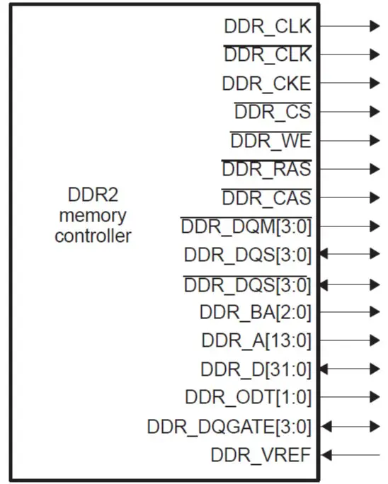
DDR2 SDRAM Memory Signal Definition
Below are the DDR2 SDRAM signals along with Direction and Active stage informationms. The number of address and data pins can vary based on the memory size and organization. Always refer to the datasheet of the specific DDR2 SDRAM device for accurate and detailed information.
|
Signal Name |
Descriptions |
Active Level |
Directions(From SDRAM Controller to Memory) |
|
CK/nCK |
Differential Clock |
On rising/Falling edge |
Output |
|
CKE |
SDRAM Clock Enable |
High |
Output |
|
CS |
SDRAM Controller Chip Select |
Low |
Output |
|
BA[1:0] |
Bank Select Signals |
NA |
Output |
|
RAS |
Row Signal |
Low |
Output |
|
CAS |
Column Signal |
Low |
Output |
|
WE |
SDRAM Write Enable |
Low |
Output |
|
D[31:0] |
Data Bus |
NA |
Bidirectional |
|
A[13:0] |
Address Bus |
NA |
Output |
|
DQM(3:0) |
Data Mask |
On rising/Falling edge |
Output |
|
DQS(3:0)/ nDQS(3:0) |
Differential data strobe |
NA |
Bidirectional |
|
DDR_ODT[1:0] |
On-die termination |
HIGH |
Output |
|
VDD |
Power supply (for the internal circuit) |
NA |
Power |
|
VSS |
Ground (for the intimae circuit) |
NA |
Power |
|
VDDQ |
DQ power supply |
NA |
Power |
|
VREF |
Referential voltage |
NA |
Power |
DDR2 SDRAM Memory Interface
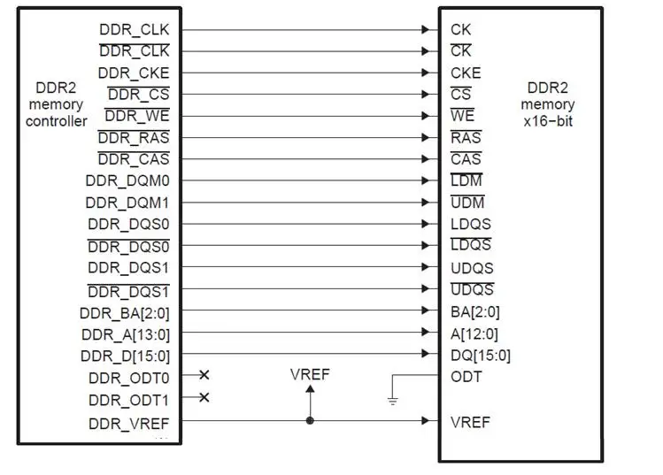
An example of interfacing 16-bit DDR2 SDRAM with MPU(16-bit wide configuration) is shown in below picture.
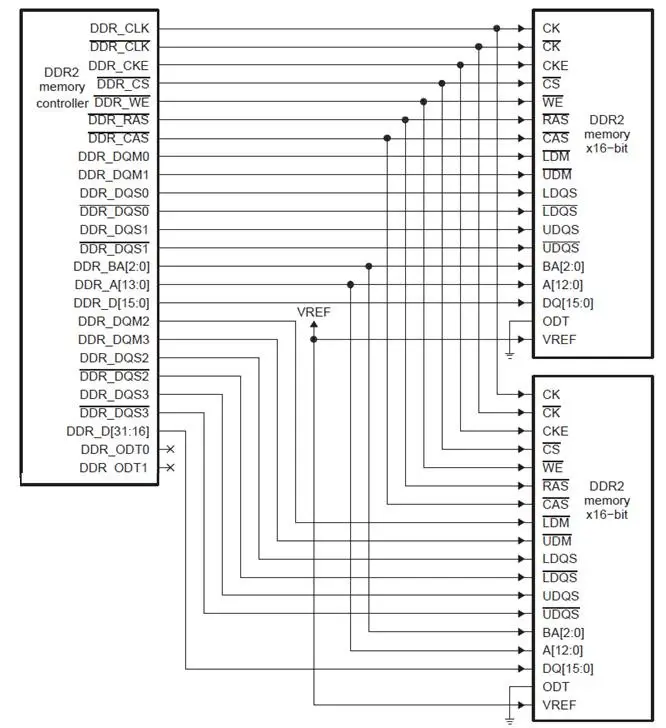
An example of interfacing Two 16-bit DDR2 SDRAM with MPU(32-bit wide configuration) is shown in below picture.
DDR2 SDRAM Signal Descriptions
DDR2 SDRAM devices use several signals for control and data transfer. Few of the key DDR2 SDRAM is as below:-
CK, nCK(System Clock): DDR2 SDRAM differential Clock, samples data on rising/falling edge. This is the primary clock signal from the DDR2 SDRAM controller to memory that controls the timing and synchronizes the operation of all DDR2 SDRAM operations. All address and control input signals are
sampled on the crossing of the positive edge of CK and negative edge of CK#. Output data (DQ and DQS/DQS#) is referenced to the crossings of CK and CK#.
CKE: DDR2 SDRAM Clock Enable. CKE signal, when registered HIGH, activates the clocking circuitry, and when registered LOW, deactivates it. CKE LOW enables precharge power-down, SELF REFRESH (all banks idle), or ACTIVATE power-down (row active in any bank). CKE is synchronous for power-down entry/exit, output disable, and self-refresh entry, and asynchronous for self-refresh exit. Input buffers (excluding CK, CK#, CKE, and ODT) are disabled during power-down.
Input buffers (excluding CKE) are disabled during self refresh.CKE is an SSTL_18 input, detecting LVCMOS LOW after VDD during the first power-up. VREF stability is crucial for proper CKE receiver operation and SELF REFRESH, needing maintenance after becoming stable during the power-on sequence.
CS (Chip Select): The Chip Select signal is used to enable (sampled LOW) or disable (sampled 1GH) the SDRAM device. When active (typically low), command input is valid & DDR2 SDRAM responds to commands and data. When the CS signal is high, all commands are ignored but the operation continues.
DQ [31:0] (Data In/Out): The DQ input/output Data Bus signals for reading from and writing to the memory are synchronized with the positive and negative edges of CLK. The IOs are byte-makeable during Reads and Writes
A(n:0)- Address bus A(n:0) are sampled during the ACTIVE command and READ/WRITE command with A10 defining auto precharge to select one location out of the memory array in the respective bank.
The number of address lines than need to be sampled depends upon memory configurations 4-Bits, 8-Bits, 16-Bits, or 32-Bits, with which memory is interfaced with a processor. A10 is sampled during a PRECHARGE command to determine whether all banks are to be recharged (A10 HIGH) or the bank selected by BA (1.0) [A1 LOW).
LDM, UDM, DM (Data Mask): In DDR2 memory, the DM (Data Mask) signal serves as an input mask for write data. When DM is sampled HIGH along with input data during a WRITE access, the corresponding data is masked.
The sampling of DM occurs on both edges of DQS (Data Strobe). While DM balls are input-only, their loading is designed to match that of DQ (Data) and DQS balls, ensuring consistent performance. Additionally, the terms LDM and UDM refer to DM signals for the lower byte (DQ[7:0]) and upper byte (DQ[15:8]), respectively.
ODT (On-die termination): In DDR2 SDRAM, the ODT (On-Die Termination) signal, when registered HIGH, activates termination resistance internally. This termination is selectively applied to specific balls based on the memory configuration: for x16, it includes DQ[15:0], LDM, UDM, LDQS, LDQS#, UDQS, and UDQS#; for x8, it involves DQ[7:0], DQS, DQS#, RDQS, RDQS#, and DM; and for x4, it applies to DQ[3:0], DQS, DQS#, and DM. It’s important to note that the ODT input can be ignored if disabled via the LOAD MODE command.
Data strobe signal (DQS, DQS#): Data Strobe (DQS) serves different roles based on the operation. For read operations, it is an output for read data, and for write operations, it is an input with the write data. In source synchronous operation, the DQS is edge-aligned with the read data and center-aligned with the write data. It’s important to note that DQS# is utilized only when the differential data strobe mode is enabled through the LOAD MODE command.
CAS (Column Address Strobe): The Column Address Strobe CAS# is an active low command signal issued by the DDR2 SDRAM controller to DDR2 SDRAM Memory. It is issued within conjunction with the RAS# and signals and is latched at the positive edges of CLK. Different signal levels of RAS, CAS. WE and CS SDRAM controller issues different types of commands to SDRAM to perform different operations.
RAS (Row Address Strobe): The row address strobe RAS# is an active low command signal issued by DDR2 SDRAM controller to DDR2 SDRAM Memory. It is issued in conjunction with the CAS# and WE signals and is latched at the positive edges of CLK. Different signal levels of RAS, CAS. WE and CS, DDR2 SDRAM controller issues different type of commends to DDR2 SDRAM Memory to perform different operations.
WE (Write Enable): The Write Enable signal WE is an active low command signal issued by DDR2 SDRAM controller to DDR2 SDRAM Memory. It is issued in conjunction with RAS and CAS signals and is latched at the positive edges of CLK. The WE# input is used to select the BankActivate or Precharge command and Read or Write command.
BAn (Bank Address): The Bank Address issued by DDR2 SDRAM controller to DDR2 SDRAM Memory. These signals specify which bank within the DDR2 SDRAM is being accessed. It define to which bank an ACTIVATE, READ, WRITE, or PRECHARGE command is being applied. BA[2:0] define which mode register, including MR, EMR, EMR(2), and EMR(3), is loaded during the LOAD MODE command.
DDR2 SDRAM Functional Description
The DDR2 SDRAM employs a double data rate architecture with a 4n-prefetch design, enabling the transfer of two data words per clock cycle at the I/O balls. A single READ or WRITE operation consists of a 4n-bit-wide, two-clock-cycle data transfer internally and four corresponding n-bit-wide, one-half-clock-cycle data transfers externally.
The bidirectional data strobe (DQS, DQS#) is transmitted externally with data, edge-aligned for READs, and center-aligned for WRITEs. For x16 configurations, separate data strobes (LDQS, LDQS#, UDQS, UDQS#) are provided for the lower and upper bytes.
Operated by a differential clock (CK and CK#), commands are registered at every positive edge of CK, while input data is registered on both edges of DQS, and output data is referenced to both edges of DQS and CK. Read and write accesses are burst-oriented, initiated by ACTIVATE commands followed by READ or WRITE commands, using registered address bits.
Programmable burst lengths of four or eight locations are supported, and interruptions with auto precharge can be enabled. The pipelined, multibank architecture allows concurrent operation, enhancing effective bandwidth.
DDR2 SDRAM features self-refresh and power-down modes, with all inputs compatible with JEDEC standard SSTL_18. The outputs, with full drive strength, are also SSTL_18-compatible, providing a balance between high performance and power efficiency.
DDR2 SDRAM Addressing
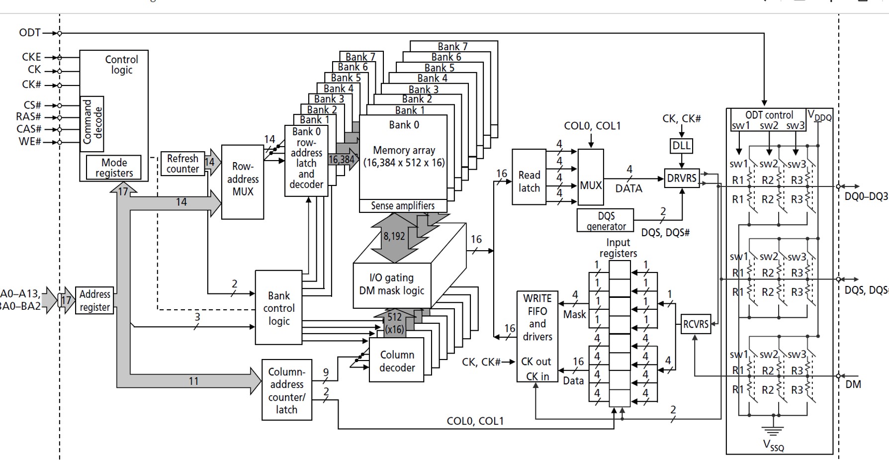
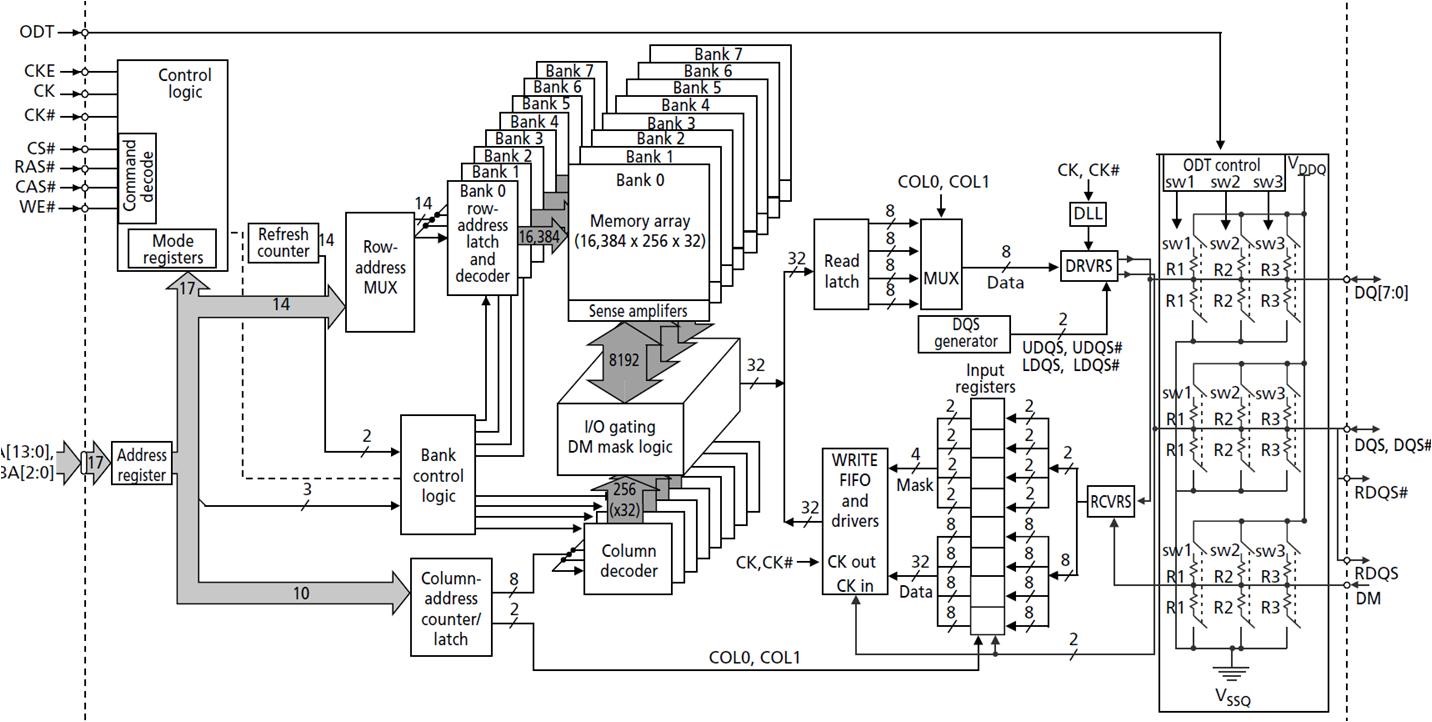
Functional Block Diagrams 1Gb: x4, x8, x16 DDR2 SDRAM
Addressing:-
|
Parameter |
256 Meg x 4 |
128 Meg x 8 |
64 Meg x 16 |
|
Configuration |
32 Meg x 4 x 8 banks |
16 Meg x 8 x 8 banks |
8 Meg x 16 x 8 banks |
|
Refresh count |
8K |
8K |
8K |
|
Row address |
A[13:0] (16K) |
A[13:0] (16K) |
A[12:0] (8K) |
|
Bank address |
BA[2:0] (8) |
BA[2:0] (8) |
BA[2:0] (8) |
|
Column address |
A[11, 9:0] (2K) |
A[9:0] (1K) |
A[9:0] (1K) |
Functional Block Diagram:- 256 Meg Locations x 4-Bits Bus
Memory calculations for above memory DDR2 SDRAM organizations:-
Data Bus Width = 4-Bits
No of Row Address Bits: – 14
No of Column Address Bits: – 11
No of Banks = 8
Total number of Memory locations in the DDR2 SDRAM=
2^No of Row Address Bits x 2^ No of Column Address Bits x No of Banks
= 2^14 x 2^ 11 x 8 = 2^14 x 2^ 11 x 2^3 = 2^28 =256 Mega locations
Total Size of DDR2 SDRAM memory =
Data Bus Width x Total number of Memory locations in the DDR2 SDRAM
= 4- bit x 128 Mega locations = 1Gb
Functional Block Diagram:- 128 Meg Locations x 8-Bits Bus
Memory calculations for above memory DDR2 SDRAM organizations:-
Data Bus Width = 8-Bits
No of Row Address Bits: – 14
No of Column Address Bits: – 10
No of Banks = 8
Total number of Memory locations in the DDR2 SDRAM=
2^No of Row Address Bits x 2^ No of Column Address Bits x No of Banks
= 2^14 x 2^ 10 x 8 = 2^14 x 2^ 10 x 2^3 = 2^27 = 128 Mega locations
Total Size of DDR2 SDRAM memory =
Data Bus Width x Total number of Memory locations in the DDR2 SDRAM
= 8-Bits x 618 Mega locations = 1Gb
Functional Block Diagram:- 64 Meg Locations x 16-Bits Bus
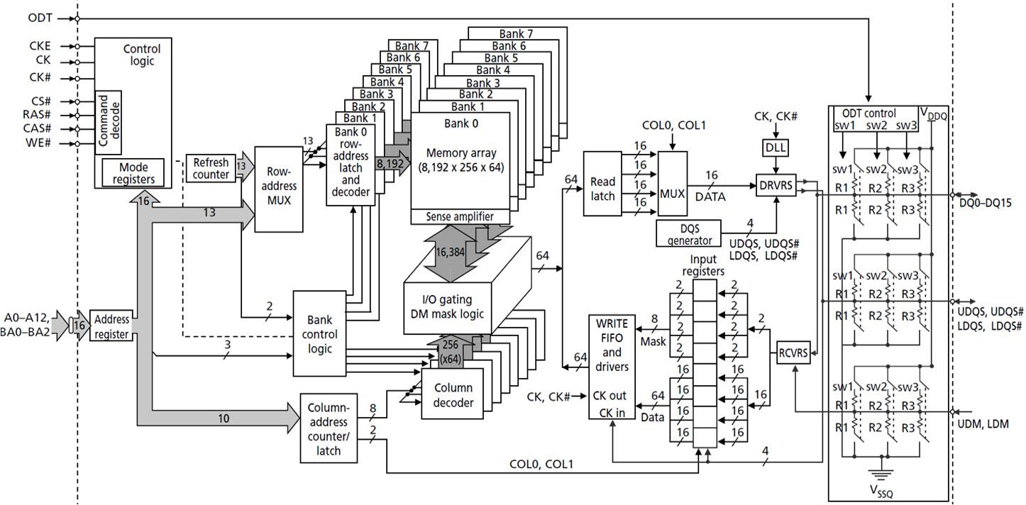
Memory calculations for above memory DDR2 SDRAM organizations:-
Data Bus Width = 16-Bits
No of Row Address Bits: – 13
No of Column Address Bits: – 10
No of Banks = 4
Total number of Memory locations in the DDR2 SDRAM=
2^No of Row Address Bits x 2^ No of Column Address Bits x No of Banks
= 2^13 x 2^ 10 x 8 = 2^13 x 2^10 x 2^3 = 2^26 = 64 Mega locations
Total Size of DDR2 SDRAM memory =
Data Bus Width x Total number of Memory locations in the DDR2 SDRAM
= 16-Bits x 64 Mega locations = 1Gb
Summary
In summary, interfacing DDR2 SDRAM involves careful consideration of specifications, proper signal connections, power distribution, and thorough testing for optimal performance. Compliance with standards and documentation of design details are essential for a successful interface.
- DDR2 Memory Controller:
- Compliant with JESD79D-2A standard.
- Facilitates communication between processors and DDR2 SDRAM devices.
- Supports seamless interface through a glueless connection.
- ODT Functionality:
- On-Die Termination (ODT) addresses signal reflection.
- Incorporates termination resistance in DRAM.
- Activates termination resistance on data I/O pins, data strobe signals, and write data mask signals.
- Interface Steps:
- Select a compatible MPU/FPGA/Controller.
- Understand DDR2 specifications, referring to the datasheet.
- Follow guidelines for clocking, address, and command signal connections.
- Pay attention to data bus routing with a focus on signal integrity.
- Power and Ground:
- Provide stable power and ground connections to DDR2 SDRAM.
- Ensure proper power distribution for reliable operation.
- Termination and Impedance Matching:
- Implement termination resistors and impedance matching.
- Optimize signal integrity, reducing signal reflections.
- Calibration and Training:
- Consider calibration and training algorithms supported by the DDR2 controller.
- Fine-tune signal parameters for optimal performance.
- Rigorous Testing:
- Use simulation tools and hardware debuggers for thorough testing.
- Verify correct operation of read and write accesses, timing requirements, and system stability.
- Documentation:
- Document design details, referring to datasheets for specific guidelines.
- Include signal connections, timing parameters, and any specific configurations.
- DDR2 SDRAM Signal Descriptions:
- Key signals include CK (Differential Clock), CKE (Clock Enable), CS (Chip Select), BA (Bank Select), RAS (Row Signal), CAS (Column Signal), WE (Write Enable), DQ (Data Bus), A (Address Bus), DQM (Data Mask), DQS (Data Strobe), ODT (On-die Termination), and power-related signals.
- Functional Description:
- DDR2 SDRAM uses a double data rate architecture with a 4n-prefetch design.
- Read and write operations are burst-oriented.
- Features self-refresh and power-down modes.
- Operates with a differential clock and supports concurrent operation for high effective bandwidth.
- Addressing and Memory Configurations:
- DDR2 SDRAM configurations illustrated for 256 Meg x 4, 128 Meg x 8, and 64 Meg x 16.
- Parameters include row address bits, column address bits, number of banks, and refresh count.
Author Profile
- 20+ years embedded hardware design professional with a burning passion for teaching. Sharing the intricate world of embedded hardware is my mission and joy.
Latest entries
 Tech Updates30 November 2025STM32WBA6: The Next-Generation MCU Powering Secure Short-Range Wireless Designs
 Blogs24 November 2025High-Speed PCB Layout Design Guide-104
 Tech Updates14 September 2025Renesas Launches RL78/L23 Ultra-Low-Power MCUs to Power Smarter Home Appliances
 Blogs7 September 2025High-Speed PCB Layout Design Guide-103