DDR2 SDRAM (Double Data Rate 2 Synchronous Dynamic Random-Access Memory), represents a significant advancement over DDR SDRAM, focusing on enhanced performance and increased bandwidth. Achieving higher data transfer rates through efficient clock cycle utilization, DDR2 provides elevated memory bandwidth, delivering more data per second. Operating at lower voltages, it reduces power consumption and supports higher memory capacities on a single module.
While not backward compatible with DDR, DDR2 memory controllers and motherboards are designed to accommodate both DDR and DDR2 modules. The evolution of memory technology is evident as DDR2 has been succeeded by subsequent generations such as DDR3, DDR4, and DDR5, each introducing further improvements.
DDR2’s features go beyond the DDR SDRAM specification, operating at data rates of 800 Mbps and above, and incorporating changes in DRAM architecture, signaling, and mode register enhancements for lower power and improved command/data bandwidth. This dynamic evolution underscores the continuous progress in memory technology.
Also Read: WHAT IS DDR SDRAM MEMORY?
Specification of DDR2 Vs SDR SDRAM Memory
|
Parameters |
DDR2 SDRAM |
DDR SDRAM |
|
Typical Operating Voltage |
1.8V |
2.5V |
|
I/O Voltage |
1.8V |
2.5V |
|
Densities |
256Mb–2Gb |
64Mb–1Gb |
|
I/O Width |
x4/ x8/ x16 |
x4/ x8/ x16 |
|
Prefetch Architecture |
4N |
2N |
|
input/output logic level |
STL_18 |
SSTL_2-compatible |
|
/CAS Latency(CL) |
3, 4, 5, 6 clocks |
2-2.5,3 Clock cycle |
|
Additive Latency (AL) |
0, 1, 2, 3, 4 clocks |
NO |
|
/CAS write latency |
READ latency – 1 clock |
1 Clock cycle |
|
/CAS Read latency |
AL + CL |
CL |
|
Clock Speed(Internal) |
200, 266, 333, 400 MHz |
100, 133, 166, 200 MHz |
|
Data Rate |
400, 533, 667, 800 Mbps |
200, 266, 333, 400 Mbps |
|
Burst Length |
4,8 |
2, 4, 8 |
|
Data Strobe |
Bidirectional strobe (single ended or differential) with RDQS |
Bidirectional strobe (single ended) |
|
Package |
FBGA only |
TSOP and FBGA |
Functionality of DDR2 VS. DDR SDRAM
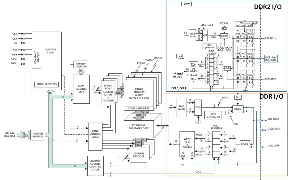
The comparison of the functional block diagrams for the 32 Meg x 16 DDR2 and DDR memory indicates a fundamental similarity in the memory core structure, as illustrated in above Figure. Despite potential differences in their operational aspects, the core components and organization of the memory appear to align closely between DDR and DDR2 configurations.
DDR and DDR2 SDRAM share an identical addressing and command control interface, a four-bank memory array, and common refresh requirements. However, DDR2 introduces key enhancements, including On Die Termination (ODT) in the IO structure. Architectural changes in DDR2 involve a shortened page size for reduced activation power, burst lengths of four and eight for improved data bandwidth, and the addition of eight banks in 1Gb densities and above.
DDR2 SDRAM can prefetch data in a 4×n-bit width without requiring a higher internal bus frequency. Notably, DDR2 operates at twice the external clock frequency of DDR SDRAM, enabling it to transfer data four times faster than SDR SDRAM and operate at twice the frequency of DDR SDRAM, resulting in significantly improved performance.
New Features of DDR2 SDRAM
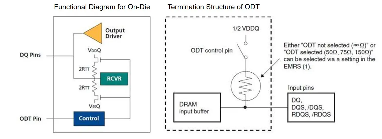
Concept of On-die Termination (ODT)
On-die termination (ODT) is a feature added to DDR2 data signals to enhance signal integrity within the system. The functional diagram of on-die termination is illustrated in below Figure. The termination value, represented by RTT, is the Thevenin equivalent of resistors that terminate the DQ inputs to VSSQ and VDDQ.
An ODT pin is incorporated into the DRAM, allowing the system to control the activation and deactivation of termination as needed. In a straightforward system with a single DRAM load per DQ signal, the termination is activated during WRITE operations and disabled during READ operations, providing a flexible mechanism to optimize signal termination based on the specific requirements of the data transfer.
DDR2 SDRAM utilizes the On-Die Termination (ODT) control pin to set the termination resistance simultaneously for various signals, including DQ, DQS, /DQS, RDQS, and /RDQS. This ODT control pin allows the system to activate or deactivate the termination resistance for these signals collectively, optimizing signal integrity and performance during different memory operation phases.
4-Bit Prefetch Architecture
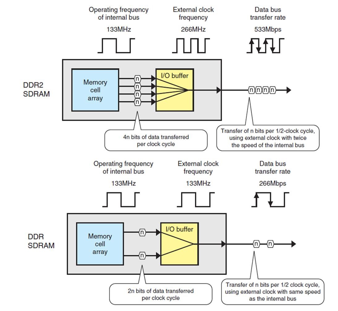
The prefetch operation in DDR2 SDRAM involves fetching data from the memory cell array into an I/O buffer in advance of its actual transfer. This is particularly advantageous when the operating speed of the I/O buffer exceeds that of the memory cell array, allowing DRAM to increase the volume of data transferred in a single clock cycle during the prefetch operation. DDR2 SDRAM specifically employs the 4-bit prefetch method, contributing to its enhanced data transfer efficiency.
DDR SDRAM having the same operating frequency as SDR SDRAM, DDR SDRAM is capable of transferring data at twice the speed. It achieves this by utilizing a prefetch function, latching data in a 2×n-bit width from the memory cell array to the I/O buffer at the same operating frequency as the external clock, securing a larger data transfer area without requiring a higher internal bus frequency.
DDR2 SDRAM further advances this concept by operating at twice the frequency of DDR SDRAM. This allows DDR2 SDRAM to prefetch data in a 4×n-bit width (4-bit prefetch) without necessitating a higher internal bus frequency. This increased efficiency in data transfer contributes to improved overall performance in DDR2 SDRAM compared to its predecessors.
DDR2 Page Size
The page size of a Synchronous Dynamic Random Access Memory (SDRAM) device plays a major role in its power consumption. It is defined as the minimum number of column locations accessed with a single ACTIVATE command. This is determined by multiplying the number of column locations by the number of DQs (Data Queues) on the DRAM. For instance, a 512Mb, x8 DDR2 SDRAM with 1,024 column locations results in a page size of 8,192 bits, which is 1,024 bytes or 1KB when divided by a word length of 8.
During an ACTIVATE command, all bits in the page are read and restored, contributing significantly to active power. A shorter page size, such as that of the 512Mb DDR2 device, compared to DDR SDRAM, reduces operating current during ACTIVATE commands, leading to improved IDD0, IDD1, and IDD7 specifications and overall lower power consumption. Refer to Table 1 for a comparison of DDR2 and DDR page sizes and banks.
|
Density |
DDR2 |
DDR |
|
|
256Mb |
Page Size |
1KB |
1KB |
|
Banks |
4 |
4 |
|
|
512Mb |
Page Size |
1KB (x4, x8), 2KB (x16) |
2KB |
|
Banks |
4 |
4 |
|
|
1Gb |
Page Size |
1KB (x4, x8), 2KB (x16) |
2KB |
|
Banks |
8 |
4 |
|
|
2Gb |
Page Size |
1KB (x4, x8), 2KB (x16) |
– |
|
Banks |
8 |
– |
|
In higher-density DDR2 SDRAM modules, such as the 512Mb, 1Gb, and 2Gb versions, the page size increases for x16 devices. However, x4 and x8 devices maintain a 1KB page size, similar to the 256Mb DDR2 SDRAM. While the x16 DDR2 page size increases to 2KB, the power consumption on x16 devices rises. Nevertheless, the overall system power is typically not higher than that of the x8 device.
This is because a 64-bit bus requires eight x8 DRAM devices, while only four x16 DRAM devices are needed. Consequently, although the activate current of a x16 component may be somewhat higher, the overall system power consumption remains lower.
DDR2 Bank Accesses
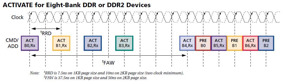
One notable change from DDR to DDR2,is number of banks for larger-density DDR2 devices. A typical four-bank access, applicable to 256Mb and 512Mb DDR2 SDRAM, is illustrated in below Figure, Bank accesses for DDR2 devices is as same as DDR, but with ACTIVATE command spacing of 7.5ns for 1KB and 10ns for 2KB page sizes due to the increased power consumption of the larger page size. After a bank is precharged, it can be activated again following the original ACTIVATE command once tRC is met.
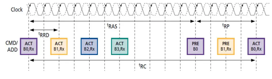
In the case of larger-density 1Gb and 2Gb DDR2 devices, eight banks are utilized, enhancing flexibility in DRAM accesses. However, this also increases the power demand on the DRAM. To prevent adverse effects on DRAM functionality and the memory subsystem due to power delivery, an additional restriction (tFAW) is imposed on bank ACTIVATE commands, as depicted in Figure 2. While ACTIVATE-to-ACTIVATE spacing remains at tRRD, an additional constraint within any tFAW window stipulates that no more than four banks may be activated. This necessitates a brief delay before activating the fifth bank.
DDR2 CAS Latency
DDR2 operates at higher clock frequencies than DDR SDRAM. As clock rates increase, the number of latencies possible must also increase. The DRAM latency is calculated as tCK × CAS latency supported.
DDR2 is targeted for latencies of 12ns–20ns. If the DRAM latency is beyond this range, it is unlikely that a system will utilize that latency due to lost system performance. Likewise, it is unlikely the DRAM will meet latencies below 12ns due to DRAM core performance. To support DDR2’s higher clock rates, the CAS latency programmability has been set at three to six clocks. Half clock latencies are not supported.
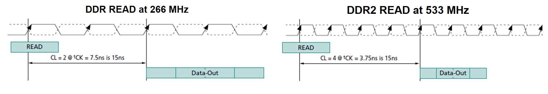
Take an example of DDR READ orations at a 266 MHz data rate and a DDR2 READ at a 533 MHz data rate. The latency of each device is the same, approximately 15ns that is two clock cycle for DDR SDRAM, this is equivalent to; four clock for DDR2.
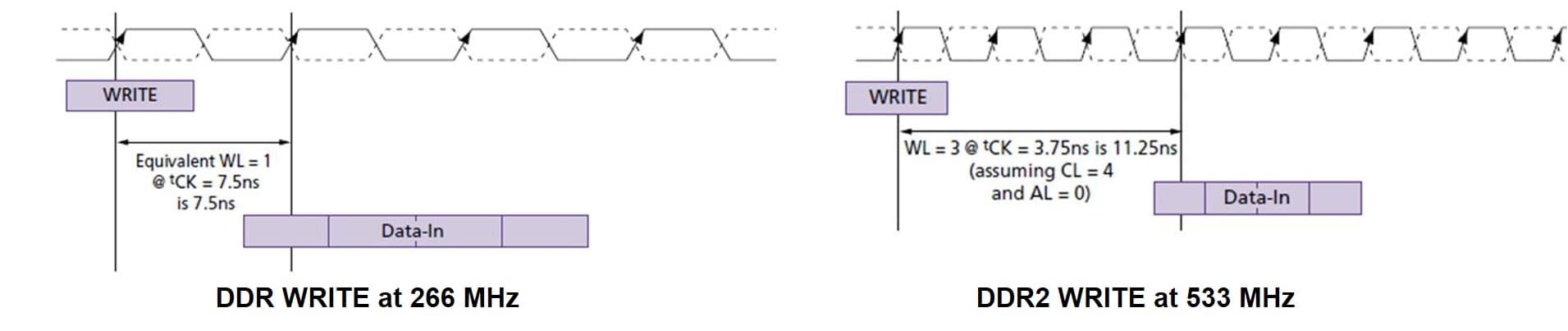
DDR2 vs. DDR READ/WRITE Latency
DDR2 includes a modification to the READ/WRITE latency specification. Below figure illustrates the differences between DDR and DDR2 SDRAM READ/ WRITE latency.
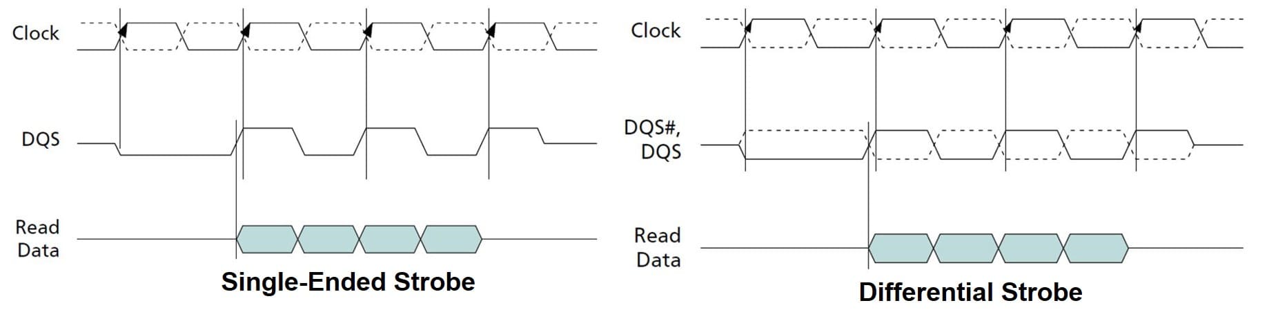
Data strobe signal (DQS)
DDR2 SDRAM supports both single-ended and differential strobes. In single-ended mode, the Data Strobe (DQS) operates conventionally. However, when differential strobes are enabled, DQS operates similarly to single-ended mode, but with the addition of DQS# acting as the complement in differential signals.
During READ operations, the DRAM outputs both signals, while for WRITE operations; both input signals must be provided by the system. The adoption of differential strobes is system-dependent and may offer improved system timings by mitigating crosstalk and reducing simultaneous switching noise on the strobe output drivers. This flexibility in strobe configurations allows for optimization based on the specific requirements and considerations of the system architecture.
DDR2 SDRAM Commands
In DDR2 SDRAM (Double Data Rate Synchronous Dynamic Random Access Memory), the memory controller communicates with the memory module by issuing commands at the rising edge of the clock signal (CK). The rising edge of the clock signal is used as a reference point for the timing of commands and data transfers. This synchronous operation ensures that data is transferred and commands are executed in a coordinated manner, enhancing the overall efficiency and reliability of the memory system.
DDR2 SDRAM (Synchronous Dynamic Random-Access Memory) commands and their meanings are provided as below. These commands are essential for controlling the operation and data access of DDR2 SDRAM devices. Here’s a summary of these commands and their functions:
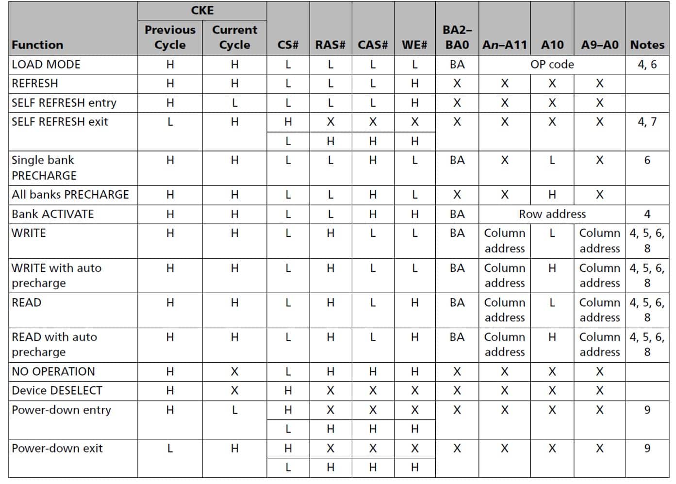
The DDR2 SDRAM operates through a series of defined command states, each serving a specific function in the memory access process:
DDR2 SDRAM READ
The DDR2 SDRAM READ command initiates a burst read access to an active row. Bank selection is determined by the bank address inputs, and the starting column location is specified by address inputs A0–A1. The A10 input determines auto precharge, with precharging occurring at the end of the read burst if selected. DDR2 supports the AL feature, enabling READ or WRITE commands before tRCD by delaying registration through AL clock cycles. Understanding these aspects is crucial for efficient memory access in DDR2 SDRAM systems.
DDR2 SDRAM WRITE
The DDR2 SDRAM WRITE command initiates a burst write access to an active row. It involves selecting the bank, specifying the starting column location, and determining auto precharge. DDR2 supports the AL feature, enabling READ or WRITE commands before tRCD by delaying registration. During WRITE, data on DQ is written based on DM input logic; LOW allows writing, HIGH ignores the data. Reference to Figure 66 provides further insight into DM input logic and the WRITE operation. Understanding these aspects is essential for efficient memory access in DDR2 SDRAM systems.
PRECHARGE Command in DDR2 SDRAM
The PRECHARGE command in DDR2 SDRAM deactivates the open row in a bank or all banks. The bank becomes available for a subsequent row activation after a specified time (tRP), unless concurrent auto precharge is enabled. In the latter case, a READ or WRITE command to a different bank is allowed without interrupting the data transfer in the current bank, as long as timing parameters are not violated. After precharging, the bank is in the idle state and must be activated before issuing READ or WRITE commands. A PRECHARGE command is permitted if the bank is in the idle state or if the previously open row is already in the process of precharging, with the precharge period determined by the last PRECHARGE command issued to the bank.
REFRESH in DDR2 SDRAM
REFRESH in DDR2 SDRAM, similar to CAS#-before-RAS# (CBR) REFRESH, is employed during normal operation. All banks must be in idle mode before issuing a REFRESH command. The command is nonpersistent and must be issued whenever a refresh is needed. Internal refresh controller generates addressing, making address bits irrelevant (“Don’t Care”) during a REFRESH command.
SELF REFRESH Command in DDR2 SDRAM
The SELF REFRESH command in DDR2 SDRAM preserves data during system power-down without external clocking. Activation is similar to a REFRESH command but with CKE set to LOW. The DLL is automatically disabled upon entering self-refresh and re-enabled upon exiting. Maintenance of valid power supply inputs, including Vref, is crucial during entry, exit, and the SELF REFRESH operation.
Summary:
- DDR2 SDRAM (Double Data Rate 2 Synchronous Dynamic Random-Access Memory) is an advancement over DDR SDRAM, offering increased performance and bandwidth.
- It achieves higher data transfer rates through efficient clock cycle utilization and operates at lower voltages, reducing power consumption.
- DDR2 supports higher memory capacities on a single module and is not backward compatible with DDR but can be accommodated by DDR/DDR2-compatible controllers and motherboards.
- Key features include a 4-bit prefetch architecture, on-die termination (ODT) for signal integrity, and a 1.8V operating voltage.
- Memory commands (READ, WRITE, PRECHARGE, REFRESH, SELF REFRESH) are registered at every rising edge of the clock signal (CK).
- DDR2 page sizes vary with densities, and larger-density devices introduce eight banks for enhanced flexibility in DRAM accesses.
- DDR2 introduces a 4-bit prefetch architecture, reducing operating current during ACTIVATE commands and improving power consumption.
- On-die termination (ODT) enhances signal integrity, providing control over termination resistance.
- Page size and bank accesses vary with density, optimizing performance and power consumption.
- DDR2’s CAS latency programmability ranges from three to six clocks, supporting latencies of 12ns–20ns.
- Memory commands such as READ, WRITE, PRECHARGE, REFRESH, and SELF REFRESH are crucial for efficient memory access in DDR2 SDRAM systems.
Author Profile
- 20+ years embedded hardware design professional with a burning passion for teaching. Sharing the intricate world of embedded hardware is my mission and joy.
Latest entries
 Tech Updates30 November 2025STM32WBA6: The Next-Generation MCU Powering Secure Short-Range Wireless Designs
 Blogs24 November 2025High-Speed PCB Layout Design Guide-104
 Tech Updates14 September 2025Renesas Launches RL78/L23 Ultra-Low-Power MCUs to Power Smarter Home Appliances
 Blogs7 September 2025High-Speed PCB Layout Design Guide-103