The DDR4 memory controller, adhering to the JESD79-4 standard, facilitates seamless communication between processors and DDR4 SDRAM memory devices. It establishes a glueless connection, supporting features like self-refresh mode, prioritized refresh, and customizable parameters such as refresh rate and CAS latency (Very similar to DDR3 SDRAM).
Interfacing DDR4 SDRAM with a DDR4 controller involves selecting a compatible MPU/FPGA/Controller, understanding DDR4 specifications, and interfacing the DDR4 SDRAM according to its datasheet. DDR4 SDRAM memories are available in three variants: x4, x8, and x16, representing different data widths transferred on each memory access (4 bits, 8 bits, and 16 bits, respectively).
The choice among these variants is influenced by factors such as cost, power consumption, board space, and performance requirements. Smaller data width components (e.g., x4) are generally less expensive and more power-efficient, making them suitable for applications with limited board space. In contrast, wider data width components (e.g., x8 or x16) offer higher potential data transfer rates, making them preferable for applications that prioritize performance.
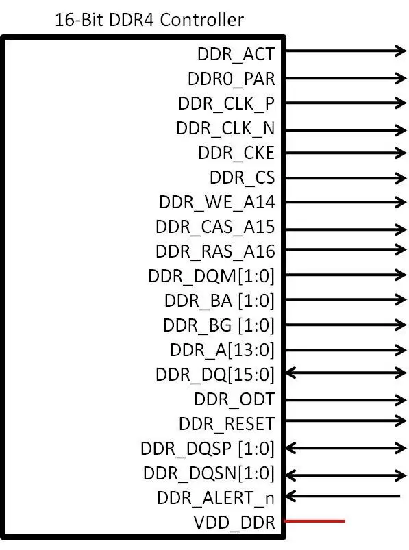
DDR4 SDRAM Memory Signal Definition
Below are the DDR4 SDRAM (16-Bits) Memory Controller signals along with Direction and Active stage information. The number of address and data pins can vary based on the memory size and organization. Always refer to the datasheet of the specific DDR4 SDRAM Controller & Memory for accurate and detailed information.
|
Pins |
Active Level |
Description |
|
DDR_DQ [15:0] |
NA |
Bidirectional data bus. Input for data reads and output for data writes. |
|
DDR_A [16:0] |
NA |
External address output from DDR4 SDRAM Controller. |
|
DDR_CS |
Low |
Active-low (output from DDR4 SDRAM Controller) chip enable for memory space. It is used to enable the DDR4 SDRAM memory device during l memory accesses.. |
|
DDR_DQM |
High |
Active-high output data mask. output from DDR4 SDRAM Controller |
|
DDR_CLK_P |
NA |
Differential clock output from DDR4 SDRAM Controller. |
|
DDR_CLK_N |
NA |
Differential clock output from DDR4 SDRAM Controller. |
|
DDR_CKE |
High |
Clock enable output from DDR4 SDRAM Controller |
|
DDR_CAS_A15 |
Low |
Active-low column address strobe. Multiplexed with Address line A15. Output from DDR4 SDRAM Controller |
|
DDR_RAS_A16 |
Low |
Active-low row address strobe. Multiplexed with Address line A16. Output from DDR4 SDRAM Controller |
|
DDR_WE_A14 |
Low |
Active-low (output from DDR4 SDRAM Controller) write enable. Multiplexed with Address line A14 |
|
DDR_DQSP |
NA |
Differential data strobe bidirectional signals. |
|
DDR_DQSN |
NA |
Differential data strobe bidirectional signals. |
|
DDR_ODT |
High |
On-die termination signal to external DDR4 SDRAM |
|
DDR_BA |
NA |
Bank-address control (output from DDR4 SDRAM Controller) |
|
DDR_BG |
NA |
Bank-Group line to select Different Banks in DDR4 SRRAM |
|
VDD_DDR |
NA |
DDR4 Memory Controller voltage. This voltage must be supplied externally. |
DDR4 SDRAM Functional Description
The DDR4 SDRAM operates as a high-speed dynamic random-access memory, internally organized into sixteen banks (four bank groups with four banks for each bank group) for x4/x8 devices, and eight banks for each bank group (two bank groups with four banks each) for x16 devices. Utilizing a double data rate (DDR) architecture, it achieves high-speed operation with an 8n-prefetch design, transferring two data words per clock cycle at the I/O pins.
Read and write accesses are burst-oriented, starting at a selected location and continuing for a burst length of eight or a chopped burst of four in a programmed sequence. The operation commences with an ACTIVE command, followed by a READ or WRITE command. For DDR4 SDRAM, the address inputs pins are used to provide the row address for ACTIVATE commands and the column address for READ/WRITE commands. When an ACTIVATE command is issued, the row address is used to select a specific row within the memory bank, making it active for subsequent READ or WRITE operations. On the other hand, READ and WRITE commands require the column address to pinpoint a specific location within the activated row for data retrieval or storage. The combination of row and column addresses allows precise addressing of individual memory locations in the respective bank.
Address bits determine the bank, row, and starting column location for the burst operation, with additional options for auto PRECHARGE and mode selection on-the-fly. Prior to normal operation, the device undergoes a predefined power-up and initialization process, covering device reset, register definition, command descriptions, and overall device operation.
Below DDR4 Component Choice Trade-Offs for different DDR4 Configurations, this helps to decide the type of configuration that need to be used for your applications.
|
Feature |
x4 |
x8 |
x16 |
Performance Implication |
|
Page size (x64) |
8 KB |
8 KB |
8 KB |
None, all are the same. |
|
Banks |
16 |
16 |
8 |
Fewer banks reduce the performance of random and multi-thread linear traffic patterns. |
|
Bank Groups |
4 |
4 |
2 |
Fewer bank groups reduces the MC’s ability to reorder and achieve “short” timing. |
|
Data Mask |
No |
Yes |
Yes |
Without data mask, any partial write requires a read-modify-write operation, reducing overall performance. |
|
tFAW |
13 ns |
21 ns |
30 ns |
Shorter tFAW improves performance of short random traffic pattern. |
|
tRRD_L |
4.9 ns |
4.9 ns |
6.4 ns |
Shorter parameter improves overall performance. |
|
tRRD_S |
3.3 ns |
3.3 ns |
5.3 ns |
Shorter parameter improves overall performance. |
DDR4 SDRAM Memory Interface
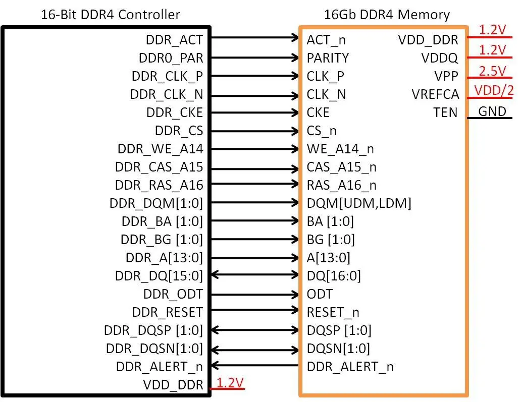
An example of interfacing Connecting one 1Gb x 16 x 8 Banks X1BG (Total Memory Size 16Gb) Devices is shown in below picture. DDR4 brings out few multiplexed pins such as pins RAS_n/A16, CAS_n/A15, and WE_n are multiplexed with A16, A15, and A14 pins respectively.
DDR4 SDRAM Signal Descriptions
DDR4 SDRAM devices use several signals for control and data transfer. Few of the key DDR4 SDRAM is as below:-
CK, nCK(System Clock) I/P: DDR4 SDRAM differential Clock input, samples data on rising/falling edge. This is the primary clock signal from the DDR4 SDRAM controller to memory that controls the timing and synchronizes the operation of all DDR4 SDRAM operations. All address and control input signals are sampled on the crossing of the positive edge of CK and negative edge of CK#. Output data (DQ and DQS/DQS#) is referenced to the crossings of CK and CK#.
CKE I/P: Clock enable, DDR4 SDRAM Clock Enable. CKE signal, Active HIGH, activates the clocking circuitry, and when registered LOW, deactivates it. CKE LOW enables precharge power-down, SELF REFRESH (all banks idle), or ACTIVATE power-down (row active in any bank). CKE is synchronous for power-down entry/exit, output disable, and self-refresh entry, and asynchronous for self-refresh exit. Input buffers (excluding CK, CK#, CKE, and ODT) are disabled during power-down. Input buffers (excluding CKE) are disabled during self refresh. VREFCA stability is crucial for proper CKE receiver operation and SELF REFRESH, needing maintenance after becoming stable during the power-on sequence.
CS (Chip Select) I/P: The Chip Select signal is used to enable (sampled LOW) or disable (sampled HIGH) the SDRAM device. When active (typically low), command input is valid & DDR4 SDRAM responds to commands and data. When the CS signal is high, all commands are ignored but the operation continues. CS# is referenced to VREFCA.
DQ[n:0](Bidirectional data bus) I/O:.The DQ input/output Data Bus signals for reading from and writing to the memory are synchronized with the positive and negative edges of CLK.
- DQ represents DQ [3:0], DQ [7:0], and DQ [15:0] for the x4, x8, and x16 configurations, respectively.
- The IOs are byte-makeable during Reads and Writes.
- Any one or all of DQ0, DQ1, DQ2, and DQ3 may be used to monitor the internal VREF level during test via mode register setting MR[4] A[4] = HIGH
A(n:0),I/P: DDR4 Address Bus. Provide the row address for ACTIVATE commands and the column address for READ/WRITE commands to select one location out of the memory array in the respective bank.
- A10 Auto PRECHARGE bit:-
- When A10 is sampled during READ and WRITE, commands determine whether auto PRECHARGE should be performed to the accessed bank after a READ or WRITE operation. (HIGH = auto PRECHARGE; LOW = no auto PRECHARGE)
- When A10 is sampled during PRECHARGE, it determines whether PRECHARGE is applied to one bank (A10 LOW) or all banks (A10 HIGH).
- Pin A12/BC_n is sampled during READ and WRITE commands to determine if burst chop (on-the-fly) will be performed. (HIGH = no burst chop; LOW = burst chopped).
- Pins A16, A15, and A14 are multiplexed with RAS_n/A16, CAS_n/A15, and WE_n/A4 functionality respectively
LDM, UDM, DM (Data Mask) I/P: In DDR4 memory, the DM (Data Mask) signal serves as an input mask for write data.
- When DM_n is sampled LOW coincident with that input data during a write access.
- DM_n is sampled on both edges of DQS (Data Strobe) & is not supported on x4 configurations.
- UDM_n and LDM_n (Upper and Lower Data Masks in x16 Configuration)
- UDM_n is associated with DQ[15:8] in the x16 configuration.
- LDM_n is associated with DQ[7:0] in the x16 configuration.
ODT (On-die termination), I/P: In DDR4 SDRAM, the ODT (On-Die Termination) signal, when registered HIGH, activates termination resistance internal to the DDR4 SDRAM. ODT (RTT) is applied selectively based on the memory configuration and enabled functions.
- x4 x8 and x16 Configurations:
- In x4 and x8 configurations, ODT is applied to each DQ, DQS_t, DQS_c, DM_n/DBI_n/TDQS_t, and TDQS_c signals.
- TDQS function must be enabled via mode register for x8 configurations.
- In x16 configuration, ODT is applied to each DQ, UDQS_t, UDQS_c, LDQS_t, LDQS_c, UDM_n, and LDM_n signals.
- The ODT pin functionality will be ignored if the mode registers are programmed to disable RTT.
Data strobe signal (DQS, DQS#), I/O: DDR4 SDRAM supports a differential data strobe only. DQS serves different roles based on the operation.
- For read operations, it is an output for read data, and for write operations, it is an input with the write data.
- In source synchronous operation, the DQS is edge-aligned with the read data and center-aligned with the write data.
- x4 x8 & x16 Configuration:
- For x4 configuration, DQS corresponds to the data on DQ[3:0].
- For x8 configuration, DQS corresponds to the data on DQ[7:0].
- For x16 configuration, LDQS corresponds to the data on DQ[7:0], and UDQS corresponds to the data on DQ[15:8].
CAS_n /A15 (Column Address Strobe) I/P: The Column Address Strobe CAS# (Multiplexed with Address line A15) is an active low command signal issued by the DDR4 SDRAM controller to DDR4 SDRAM Memory. It is issued within conjunction with the RAS# and signals and is latched at the positive edges of CLK. Different signal levels of RAS, CAS, WE and CS, DDR4 SDRAM controller issues different types of commands to DDR4 SDRAM Memory to perform different operations and are referenced to VREFCA.
RAS_n/A16 (Row Address Strobe) I/P: The row address strobe RAS# #(Multiplexed with Address line A15) is an active low command signal issued by DDR4 SDRAM controller to DDR4 SDRAM Memory. It is issued in conjunction with the CAS# and WE signals and is latched at the positive edges of CLK. Different signal levels of RAS, CAS. WE and CS DDR4 SDRAM controller issues different type of commends to DDR4 SDRAM Memory to perform different operations and are referenced to VREFCA.
WE_n/A14 (Write Enable) I/P: The Write Enable signal WE# (Multiplexed with Address line A14) is an active low command signal issued by DDR4 SDRAM controller to DDR4 SDRAM Memory. It is issued in conjunction with RAS and CAS signals and is latched at the positive edges of CLK. The WE# input is used to select the BankActivate or Precharge command and Read or Write command.
BA (n: o) (Bank Address) I/P: The Bank Address issued by DDR4 SDRAM controller to DDR4 SDRAM Memory. These signals specify which bank within the DDR4 SDRAM is being accessed. It define to which bank an ACTIVATE, READ, WRITE or PRECHARGE command is being applied.
BG (n: o) (Bank Group) I/P: The Bank Address issued by DDR4 SDRAM controller to DDR4 SDRAM Memory. DDR4 introduces the Bank Grouping feature, optimizing memory access by reducing time delays for successive accesses to different bank groups. These signal define the bank group to which an ACTIVATE, READ, WRITE, or PRECHARGE command is being applied. It also determines which mode register is to be accessed during a MODE REGISTER SET command. BG [1:0] are used in the x4 and x8 configurations. BG1 is not used in the x16 configuration.
ALERT_n O/P: This signal allows the DDR4 SDRAM Memory to indicate to the SDRAM memory controller that a specific alert or event has occurred. Alerts will include the command/ address parity error and the CRC data error. The specific alerts signalled through ALERT_n depend on the configuration and settings enabled in the mode register.
DBI_n, UDBI_n, LDBI_n I/O: DBI is a new feature introduced in DDR4, to help to improve signal integrity while reducing power consumption. DBI_n is used as an input/output signal for data bus inversion in DDR4 SDRAM.
- DBI support in different configurations:-
- In x4 Configuration DBI feature is not supported.
- In x8 configuration, DBI_n is used as an input/output signal for data bus inversion
- In x16 configuration, UDBI_n is associated with DQ[15:8], and LDBI_n is associated with DQ[7:0].
- Mode Register Settings for DBI:
- DBI, along with DM (Data Mask) and TDQS (Termination Data Strobe), can be enabled or disabled through mode register settings.
- DBI can be configured for both READ (output) and WRITE (input) operations based on the mode register settings.
TEN, I/P: TEN, Connectivity test mode input is an active HIGH signal. TEN must be LOW during normal operation. TEN is a CMOS rail-to-rail signal with DC HIGH and LOW at 80% and 20% of VDD (960mV for DC HIGH and 240mV for DC LOW).
PAR, I/P: Parity for command and address lines. This function can be selectively enabled or disabled via the mode register in DDR4 SDRAM. SDRAM Controller provides Parity information to SDRAM memory over this signal. SDRAM memory compares this information with the internally generated Parity bits and confirms if Parity error has occurred and takes appropriate actions.
- When enabled, the parity signal encompasses all command and address inputs, including ACT_n, RAS_n/A16, CAS_n/A15, WE_n/A14, A[17:0], A10/AP, A12/BC_n, BA[1:0], and BG[1:0].
- For 3DS only devices, C0, C1, and C2 are also covered with BG[1:0].
- Control pins NOT covered by the parity signal are CS_n, CKE, and ODT.
- Parity checks on command and address inputs are performed when commands are latched via the rising edge of CK_t. The checks occur when CS_n is LOW.
RESET#, I/P: RESET# input is an active LOW signal & referenced to VSSQ (ground). RESET_n must be HIGH during normal operation. It is a CMOS rail-to-rail signal with DC HIGH and LOW at 80% and 20% of VDD (960 mV for DC HIGH and 240 mV for DC LOW).
ZQ I/P: In DDR4, the ZQ (Impedance Calibration) singles is associated with output drive calibration. This Pin is connected to an external 240Ω resistor (RZQ), and this resistor is further connected to VSSQ (ground for the output buffer). The purpose of this configuration is to facilitate impedance calibration in the memory module, helping to optimize signal integrity and performance by adjusting the output drive characteristics. The external resistor tied to the ZQ singles Pins plays a role in determining the impedance values during calibration, enhancing the overall reliability of the DDR4 memory interface.
DDR4 Power Supply Signals:
- VDD Supply (Power supply): 2V +/- 0.060V.
- VDDQ Supply (DQ power supply): 2V +/- 0.060V.
- Vpp: DRAM activating power supply : 2.5V, -0.125V /+0.250V
- VREFCA Supply (Reference voltage for control, command, and address):
- Must be maintained at all times, including self-refresh, for proper device operation.
- Used as a reference voltage for control, command, and address signals.
- VSS Supply (Ground):
- Common ground reference for the entire device.
- VSSQ Supply (DQ ground):
- Isolated ground for the data input/output circuits.
- Improves noise immunity by providing a separate ground for the data paths.
DDR4 SDRAM Addressing
16Gb: x4, x8, x16 DDR4 SDRAM Addressing
|
Parameter |
4096 Meg x 4 |
2048 Meg x 8 |
1024 Meg x 16 |
|
Number of bank groups |
4 |
4 |
2 |
|
Bank group address |
BG[1:0] |
BG[1:0] |
BG0 |
|
Bank count per group |
4 |
4 |
4 |
|
Bank address in bank group |
BA[1:0] |
BA[1:0] |
BA[1:0] |
|
Row addressing |
256K (A[17:0]) |
128K (A[16:0]) |
128K (A[16:0]) |
|
Column addressing |
1K (A[9:0]) |
1K (A[9:0]) |
1K (A[9:0]) |
|
Page size1 |
512B |
1KB |
2KB |
Functional Block Diagram: – 4 Gig x 4-Bit
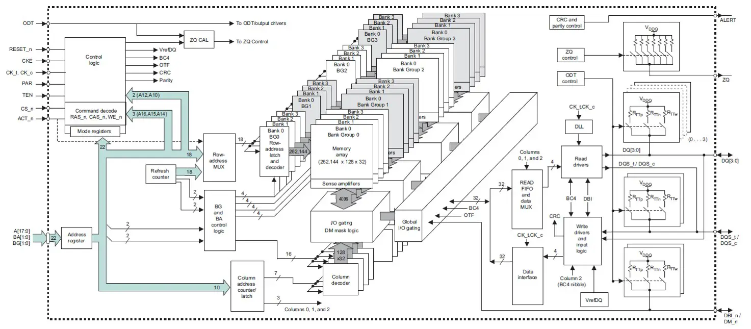
Memory calculations for above memory DDR4 SDRAM organizations:-
Data Bus Width = 4-Bits
No of Row Address Bits: – 18
No of Column Address Bits: – 10
No of Banks/ Bank Group = 4
No of Banks Group = 4
Total number of Memory locations in the DDR4 SDRAM=
2^No of Row Address Bits x 2^ No of Column Address Bits x No of Banks x No of Bank Group
= 2^18 x 2^ 10 x 4 x 4 = 2^18 x 2^ 10 x 2^2 x 2^2 = 2^32 = 4 Giga locations
Total Size of DDR4 SDRAM memory =
Data Bus Width x Total number of Memory locations in the DDR4 SDRAM
= 4- bit x 4 Giga locations = 16Gb
Functional Block Diagram: – 2 Gig x 8-Bits
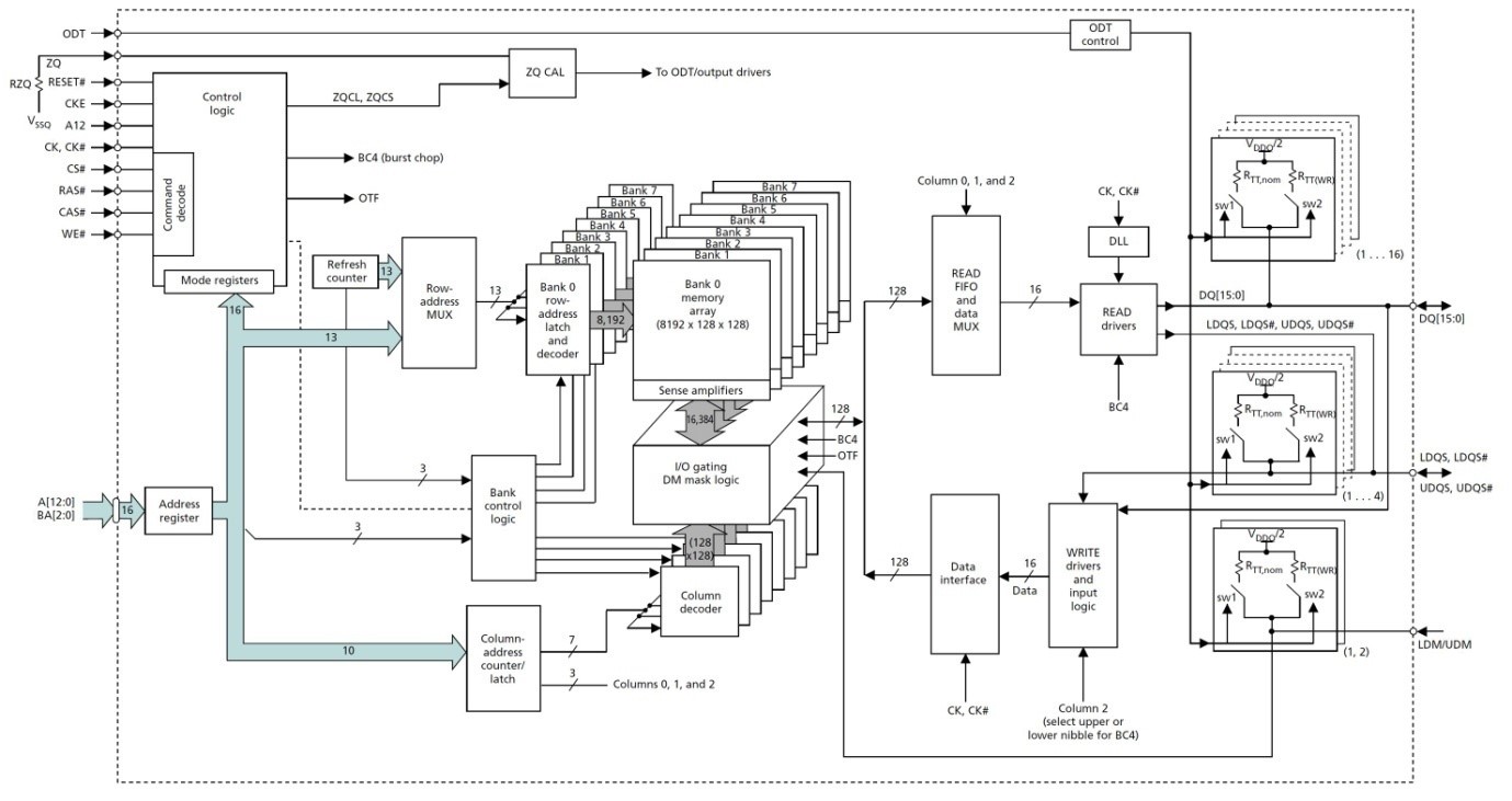
Memory calculations for above memory DDR4 SDRAM organizations:-
Data Bus Width = 8-Bits
No of Row Address Bits: – 17
No of Column Address Bits: – 10
No of Banks/ Bank Group = 4
No of Banks Group = 4
Total number of Memory locations in the DDR4 SDRAM=
2^No of Row Address Bits x 2^ No of Column Address Bits x No of Banks x No of Bank Group
= 2^17 x 2^ 10 x 4 x 4 = 2^17 x 2^ 10 x 2^2 x 2^2 = 2^31 = 2 Giga locations
Total Size of DDR4 SDRAM memory =
Data Bus Width x Total number of Memory locations in the DDR4 SDRAM
= 8- bit x 2 Giga locations = 16 Gb
Functional Block Diagram: – 1 Gig x 16-Bits
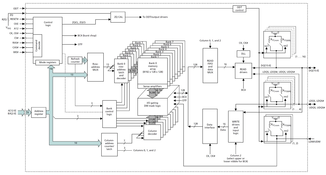
Memory calculations for above memory DDR4 SDRAM organizations:-
Data Bus Width = 16-Bits
No of Row Address Bits: – 17
No of Column Address Bits: – 10
No of Banks/ Bank Group = 4
No of Banks Group = 2
Total number of Memory locations in the DDR4 SDRAM=
2^No of Row Address Bits x 2^ No of Column Address Bits x No of Banks x No of Bank Group
= 2^17 x 2^ 10 x 4 x 2 = 2^17 x 2^ 10 x 2^2 x 2^1 = 2^30 = 1 Giga locations
Total Size of DDR4 SDRAM memory =
Data Bus Width x Total number of Memory locations in the DDR4 SDRAM
= 16- bit x 1 Giga locations = 16 Gb
Summary
In summary, interfacing DDR4 SDRAM involves careful consideration of specifications, proper signal connections, power distribution, and thorough testing for optimal performance. Compliance with standards and documentation of design details are essential for a successful interface.
- Interfacing DDR4 SDRAM Memory:
- DDR4 memory controller adheres to the JESD79-4 standard and supports features like self-refresh mode, prioritized refresh, and customizable parameters.
- DDR4 SDRAM comes in x4, x8, and x16 variants, with the choice influenced by factors such as cost, power consumption, board space, and performance requirements.
- DDR4 SDRAM Memory Signal Definitions:
- DDR4 SDRAM uses various signals like DDR_DQ, DDR_A, DDR_CS, DDR_DQM, DDR_CLK, DDR_CKE, DDR_CAS_A15, DDR_RAS_A16, DDR_WE_A14, DDR_DQSP, DDR_DQSN, DDR_ODT, DDR_BA, DDR_BG, and VDD_DDR.
- DDR4 SDRAM Functional Description:
- Operates as high-speed dynamic RAM with sixteen banks (four bank groups for x4/x8 and eight banks for x16 devices).
- Utilizes a double data rate (DDR) architecture with burst-oriented read and write accesses.
- DDR4 Component Choice Trade-Offs:
- Different configurations (x4, x8, x16) have trade-offs in page size, banks, bank groups, data mask, tFAW, tRRD_L, and tRRD_S, affecting performance in various scenarios.
- DDR4 SDRAM Signals:
- Key signals include CK (System Clock), CKE (Clock Enable), CS (Chip Select), DQ (Bidirectional data bus), A(n:0) (Address Bus), DM (Data Mask), ODT (On-die termination), DQS (Data Strobe), CAS_n/A15, RAS_n/A16, WE_n/A14, BA (Bank Address), BG (Bank Group), ALERT_n, DBI_n, UDBI_n, LDBI_n, TEN, PAR, RESET#, and ZQ.
- Multiplexed pins include RAS_n/A16, CAS_n/A15, and WE_n/A14, which are multiplexed with A16, A15, and A14 pins, respectively.
- DDR4 Power Supply Signals:
- Power supply signals include VDD, VDDQ, Vpp, VREFCA, VSS, and VSSQ, each with specific voltage requirements.
Author Profile
- 20+ years embedded hardware design professional with a burning passion for teaching. Sharing the intricate world of embedded hardware is my mission and joy.
Latest entries
 Tech Updates30 November 2025STM32WBA6: The Next-Generation MCU Powering Secure Short-Range Wireless Designs
 Blogs24 November 2025High-Speed PCB Layout Design Guide-104
 Tech Updates14 September 2025Renesas Launches RL78/L23 Ultra-Low-Power MCUs to Power Smarter Home Appliances
 Blogs7 September 2025High-Speed PCB Layout Design Guide-103