DDR4 SDRAM represents a significant improvement from its predecessor, DDR3, offering higher bandwidth, increased memory module densities, and improved signal integrity. Notable enhancements include a lower operating voltage, reduced power consumption, and on-die ECC for better error detection and correction.
With a focus on energy efficiency, DDR4 operates at 1.2V, contributing to lower heat generation. DDR4 SDRAM is internally configured as an 8-bank DRAM within a 2-Bank Group for the x16 configuration and as a 16-bank DRAM within a 4-Bank Group for the x4 and x8 configurations. The 8n-prefetch architecture is combined with an interface designed to transfer two data words per clock cycle at the I/O pins
The memory’s increased burst length, bank grouping, and optimized command bus enhance overall data access efficiency, while backward compatibility considerations ensure flexibility in system configurations. These improvements collectively make DDR4 a high-performance memory technology, particularly beneficial for applications demanding large memory capacities, increased speed, and energy efficiency.
Specification of DDR3 Vs DDR4 SDRAM Memory
|
FEATURE/OPTION |
DDR3 |
DDR4 |
DDR4 ADVANTAGE |
|
Voltage (core and I/O) |
1.5V |
1.2V |
Reduces memory power demand |
|
World Line Supply |
NA |
2.5V |
|
|
VREF inputs |
2 – DQs and CMD/ADDR |
1 – CMD/ADDR |
VREFDQ now internally genrated |
|
Low voltage standard |
Yes (DDR3L at 1.35V) |
No |
Memory power reductions |
|
IO Configurations |
x4, x8, x16 |
x4, x8, x16, x32 |
Improved data rate |
|
Data rate (Mb/s) |
800, 1066, 1333, 1600, 1866, 2133 |
1600, 1866, 2133, 2400, 2666, 3200 |
Migration to higher‐speed I/O |
|
Densities |
512Mb–8Gb |
2Gb–16Gb |
Better enablement for large-capacity memory subsystems |
|
Internal banks |
8 |
16 |
More banks |
|
Bank groups (BG) |
0 |
4 |
Faster burst accesses |
|
Address/ Command Signals |
27 pins |
29 pins (partial mux’d) |
|
|
Address/ Command Data Rate |
SDR (rising edge of clock only) |
SDR (rising edge of clock only) |
|
|
tCK – DLL enabled |
300 MHz to 800 MHz |
667 MHz to 1.6 GHz |
Higher data rates |
|
t CK – DLL disabled |
10 MHz to 125 MHz (optional) |
Undefined to 125 MHz |
DLL-off now fully supported |
|
Read latency |
AL + CL |
AL + CL |
Expanded values |
|
Write latency |
AL + CWL |
AL + CWL |
Expanded values |
|
DQ driver (ALT) |
40Ω |
48Ω |
Optimized for PtP (point-to-point) applications |
|
DQ bus |
SSTL15 |
POD12 |
Mitigate I/O noise and power |
|
RTT values (in Ω) |
120, 60, 40, 30, 20 |
240, 120, 80, 60, 48, 40, 34 |
Support higher data rates |
|
RTT not allowed |
READ bursts |
Disables during READ bursts |
Ease-of-use |
|
ODT modes |
Nominal, dynamic |
Nominal, dynamic, park |
Additional control mode; supports OTF value change |
|
ODT control |
ODT signaling required |
ODT signaling not required |
Ease of ODT control, allows non-ODT routing on PtP applications |
|
On Die Temperature Sensor |
No |
Yes |
Having ODT Temperature Sensor |
|
Drive Strength |
34-ohm 40-ohm ZQ calibration for +/-10% accuracy |
34-ohm 40-ohm TBD-ohm ZQ calibration for +/-10% accuracy |
|
|
Multipurpose register (MPR) |
Four registers – 1 defined, 3 RFU |
Four registers – 3 defined, 1 RFU |
Provides additional specialty readout |
Functional Block of DDR4 VS. DDR3 SDRAM
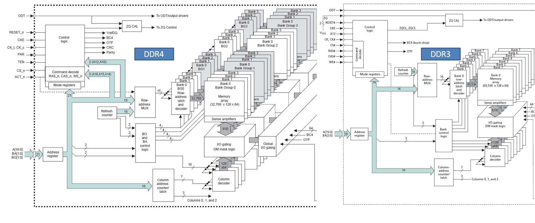
The comparison of the functional block diagrams for the 4Gb, 512 Meg x 8, DDR4 and DDR3 memory indicates a fundamental similarity in the memory core structure, as illustrated in above Figure. Despite differences in their organization of the memory, the core components, I/O driver, and operational aspects appear to align closely between DDR3 and DDR4 configurations. Internal memory of DDR3 is organized as an 8-bank, whereas for DDR4 it is configured as an 16-bank (4-banks per Bank Group). DDR4 comes with new Bank Group concept which helps in improve the access time.
While DDR4 memory systems share similarities with DDR3 counterparts, noteworthy new features, particularly improved signaling and debug capabilities, distinguish DDR4. These enhancements directly impact PCB (Printed Circuit Board) design. DDR4’s debug capabilities offer more refined tools for troubleshooting and optimizing memory performance. These changes necessitate careful consideration in PCB layout and routing to accommodate the upgraded specifications, ensuring efficient signal paths and minimizing potential interference.
DDR4 Prefetch, Clock Rate & Device Density
DDR4 uses 8n-prefetch architecture same as DDR3. At the same time, doubling the burst length to 16 would result in a “x16 device transferring 32 bytes of data” on each access, which is good for transferring large chunks of data but inefficient for transferring smaller chunks of data.
The JEDEC DDR4 standard defines clock rates up to 1600 MHz, with data rates up to 3200 Mb/s. Higher clock frequencies translate into the possibility of higher peak bandwidth.
The JEDEC® standard for DDR4 SDRAM defines densities ranging from 2–16Gb; however, the industry started production for DDR4 at 4Gb density parts.
The clock rate, data rate, prefetch lengths, and the number of banks for various SDRAM generations are tabulated below for quick reference. It can be observed that next-generation DRAM devices operate at higher clock rates and data transfer rates.
|
Product |
Clock Rate (tCK) |
Data Rate |
Density |
Prefetch |
No. of Banks |
||
|
Min |
Max |
Min |
Max |
||||
|
SDRAM |
10ns |
5ns |
100 Mb/s |
200 Mb/s |
64–512Mb |
1n |
4 |
|
DDR |
10ns |
5ns |
200 Mb/s |
400 Mb/s |
256Mb–1Gb |
2n |
4 |
|
DDR2 |
5ns |
2.5ns |
400 Mb/s |
800 Mb/s |
512Mb–2Gb |
4n |
4, 8 |
|
DDR3 |
2.5ns |
1.25ns |
800 Mb/s |
1600 Mb/s |
1–8Gb |
8n |
8 |
|
DDR4 |
1.25ns |
0.625ns |
1600 Mb/s |
3200 Mb/s |
4–16Gb |
8n |
8, 16 |
Error Detection and Data Bus Inversion
Devices operating at higher clock and data rates enable the accomplishment of more work within a given time frame. However, the increased frequencies also introduce complexity in sending and receiving information accurately. Consequently, DDR4 devices offer below features:
- Two built-in error detection modes: cyclic redundancy cycle (CRC) & Data bus inversion (DBI)
- Cyclic redundancy cycle (CRC) for the data bus and parity checking for the command and address bits.
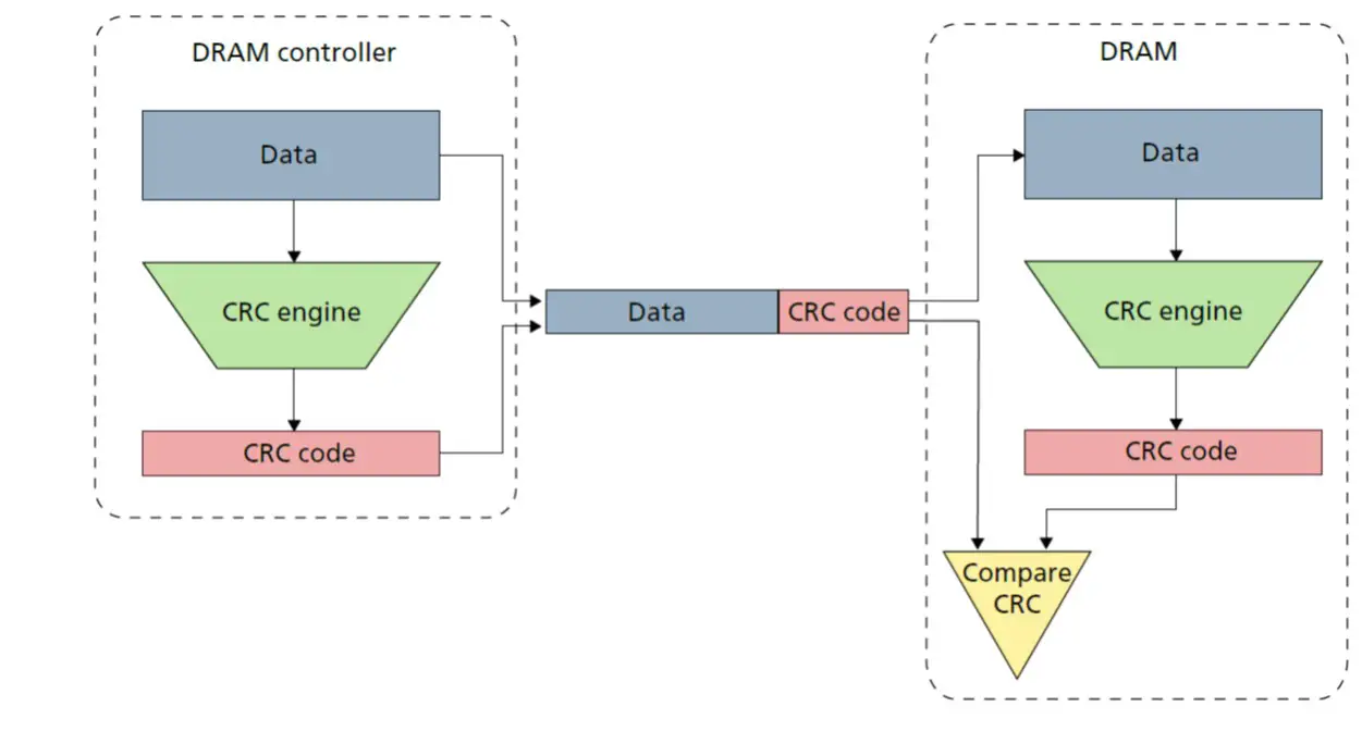
- DRAM generates a checksum for each write burst and each DQS lane, comprising 8 bits per write burst (CR0–CR7) and a CRC calculated using 72 bits of data (with unallocated transfer bits set to 1s).
- The DRAM then compares this generated checksum against the controller checksum. If the two checksums do not match, the DRAM signals an error, as illustrated in the CRC Error Detection figure.
- In the event of a CRC error, the system sets a flag using the ALERT_n signal, marked by a short low pulse lasting 6–10 clocks.
- Data bus inversion (DBI) to help improve signal integrity while reducing power consumption. A new feature introduced in DDR4, Data Bus Inversion (DBI), offers several advantages as below:-
- It is supported on x8 and x16 configurations, but not on x4 configurations.
- Configuration is set per byte: One DBI_n pin is used for x8 configuration, while UDBI_n and LDBI_n pins are used for x16 configuration.
- DBI shares a common pin with data mask (DM) and TDQS functions. Notably, Write DBI cannot be enabled simultaneously with the DM function.
- DBI inverts data bits during memory operations.
- It drives fewer bits LOW, with a maximum of half of the bits being driven LOW, including the DBI_n pin.
- This feature consumes less power, as power is only consumed by bits that are driven LOW.
- DBI enables fewer bits to switch, resulting in reduced noise and a more favorable data eye.
- It applies to both READ and WRITE operations, and each can be independently enabled or disabled, controlled by MR5 (Mode Register 5).
Concept of Banks and Bank Grouping
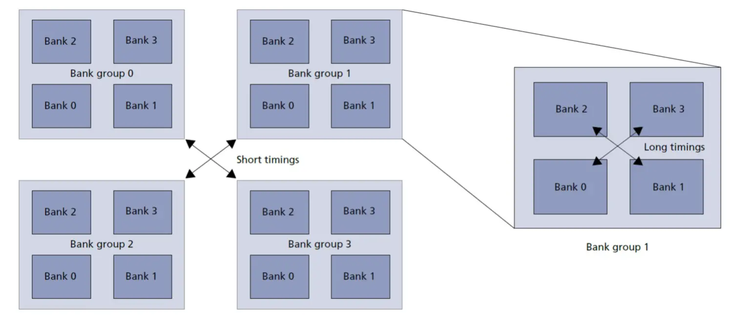
DDR4 introduces the Bank Grouping feature, optimizing memory access by reducing time delays for successive accesses to different bank groups. Shorter timing specifications between commands are permitted when accessing different bank groups, enhancing overall system performance. Conversely, accessing banks within the same group requires longer timing specifications to ensure proper coordination. This feature allows DDR4 to efficiently handle diverse memory access patterns, reducing latency for scattered accesses while maintaining integrity for consecutive accesses within the same bank group.
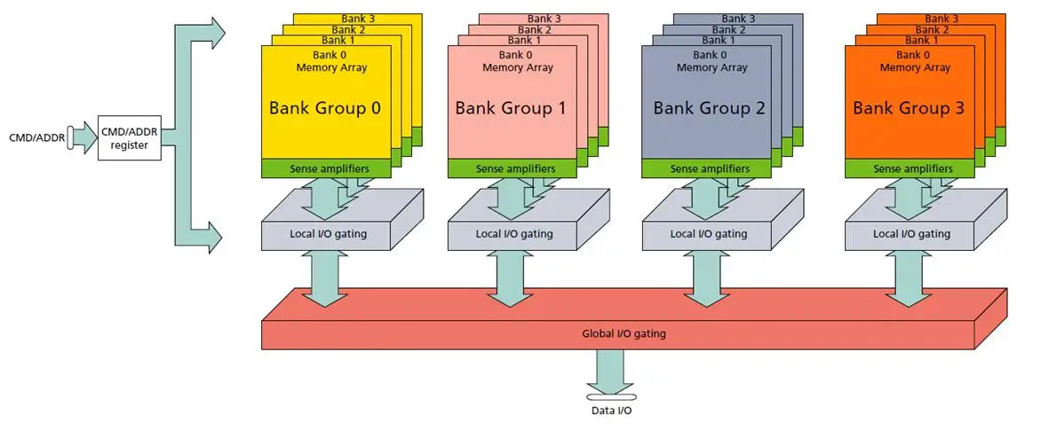
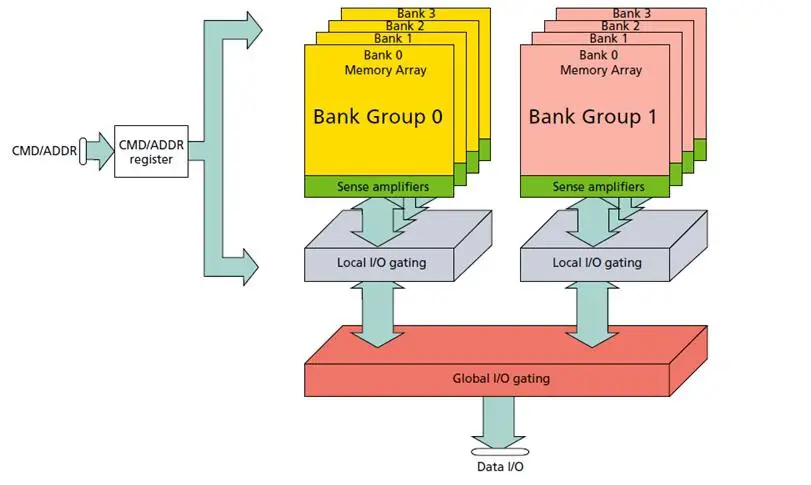
DDR4 introduces the concept of bank grouping, which varies based on the configuration of the DDR4 devices as below:-
- For x4 and x8 DDR4 devices, there are four bank groups, with each group consisting of four sub-banks.
- For x16 DDR4 devices, there are two bank groups, each comprising four sub-banks.
Bank Group: Understanding Short vs. Long Timing
In DDR4 memory architecture, “short timing” and “long timing” typically refer to the duration of specific parameters related to memory access and data transfer. Accessing different banks in different bank groups can use shorter timing specification, however when accessing banks within the same group, longer timing specifications may be required to avoid conflicts and ensure proper operation. This helps optimize memory subsystem performance by balancing timings based on the organization of memory banks.
DDR4’s Enhanced Feature’s Influence on PCB Design
New VPP supply
In DDR4 memory technology, the additions of the VPP supply a 2.5V source for the internal word line. This inclusion supports the transition of VDD from 1.5V to 1.2V and results in approximately 10% additional power savings. While JEDEC does not specify IDD and IPP current limits, initial DDR4 modules typically exhibit IPP current usage:
- 2mA to 3mA in standby mode,
- 3mA to 4mA in the active mode, and
- 10mA to 20mA during refresh mode.
These IPP values represent average currents, and the actual draw involves narrow pulses ranging from 20mA to 60mA. Failure to provide sufficient power to VPP will prevent the DRAM from operating correctly.
VREFDQ Reference Voltage Eliminations
In DDR4 memory technology, the VREFDQ reference input supply has been removed and DRAM itself internally generates VREFDQ. This change allows for flexibility, as the VREFDQ can be set to any value within a wide range. This means the DRAM controller must set the DRAM’s VREFDQ settings to the proper value; thus, the need for VREFDQ calibration.
VREFDQ Calibration Settings
In VREFDQ calibration for DDR4, we can choose between two ranges:
- Range 1: Between 60% and 92.5% of VDDQ
- Range 2: Between 40% and 77.5% of VDDQ
Range 1 is intended for module-based systems, offering flexibility for that configuration. Range 2 is designed for point-to-point-based systems. Once a range is selected, the internal VREF can be fine-tuned in 0.65% VDDQ increments to achieve the desired calibration. This customization allows for optimal settings based on the specific requirements and architecture of the system.
POD I/O Buffers
In DDR4, the I/O buffer has transitioned from push-pull to pseudo open drain (POD). Unlike before, where termination was at 1/2 VDDQ, it’s now terminated to VDDQ. This modification allows customization of the signal swing size and center according to specific design requirements. With POD, there’s a reduction in switching current when driving data, as power is consumed only when transmitting 0s. Enabling Data Bus Inversion (DBI) can lead to additional switching current savings. Furthermore, DBI brings benefits like reduced crosstalk, resulting in a larger data-eye for improved signal integrity.
ACT_n Control Pin Muxing
In DDR4, the ACT_n (Activate) control helps manage the allocation of pins by multiplexing certain address pins. This includes RAS_n/A16, CAS_n/A15, and WE_n/A14. When ACT_n is registered LOW (Active Low), DRAM treats pins RAS_n/A16, CAS_n/A15, and WE_n as /A14 as A16, A15, and A14 respectively. This state is used for latching the row address. Conversely, when ACT_n is HIGH, the inputs RAS_n/A16, CAS_n/A15, and WE_n/A14 are treated as control pins (RAS_n, CAS_n, and WE_n). This multiplexing approach allows for flexibility in pin usage based on the operational needs of the DDR4 memory system, helping to manage pin resources effectively.
Summary
- DDR4 SDRAM offers significant improvements over DDR3, with higher bandwidth, increased module densities, and improved signal integrity.
- Key features include lower operating voltage, reduced power consumption, and on-die ECC for error detection and correction.
- Operates at 1.2V, emphasizing energy efficiency, and internally configured as 8-bank DRAM with 2-Bank/4-Bank Grouping.
- The memory core structure is fundamentally similar between DDR3 and DDR4, but DDR4 introduces new features that impact PCB design and debugging capabilities.
- DDR4 uses 8n-prefetch architecture, similar to DDR3, but with a doubled burst length of 16, which is efficient for transferring large data chunks.
- The JEDEC DDR4 standard defines clock rates up to 1600 MHz and data rates up to 3200 Mb/s, offering higher peak bandwidth compared to previous generations.
- DDR4 SDRAM densities range from 2Gb to 16Gb, with initial production starting at 4Gb density parts.
- DDR4 introduces two built-in error detection modes: cyclic redundancy cycle (CRC) and Data Bus Inversion (DBI), contributing to improved accuracy in data transmission.
- Error detection includes CRC for the data bus and parity checking for command and address bits, providing robust mechanisms for identifying and addressing errors.
- DBI, a new feature in DDR4, improves signal integrity and reduces power consumption by inverting data bits during memory operations.
- Transition from push-pull to pseudo open drain (POD) I/O buffers for reduced switching current.
- Introduction of VPP supply for power savings and removal of VREFDQ reference input supply, requiring calibration.
- Bank grouping in DDR4 optimizes memory access, distinguishing short and long timing specifications for improved performance.
- ACT_n control facilitates pin multiplexing for flexible allocation between control and address pins.
- Enhanced burst length, bank grouping, and optimized command bus contribute to improved data access efficiency.
- Suitable for applications requiring large memory capacities, increased speed, and energy efficiency.
- PCB design considerations include accommodating new features like VPP supply, VREFDQ calibration, POD I/O buffers, and pin multiplexing.
Author Profile
- 20+ years embedded hardware design professional with a burning passion for teaching. Sharing the intricate world of embedded hardware is my mission and joy.
Latest entries
 Tech Updates30 November 2025STM32WBA6: The Next-Generation MCU Powering Secure Short-Range Wireless Designs
 Blogs24 November 2025High-Speed PCB Layout Design Guide-104
 Tech Updates14 September 2025Renesas Launches RL78/L23 Ultra-Low-Power MCUs to Power Smarter Home Appliances
 Blogs7 September 2025High-Speed PCB Layout Design Guide-103