Before delving into “On-Die Termination”, let’s first try to understand the concept of “Terminations”. Why is termination necessary?
High speed, rapid data transfer rates, swift response, and real-time capabilities are a few expectations from electronic devices. These collective expectations drive the necessity for electronic devices to not only function at high speeds but also to provide quick responses and real-time performance, meeting the dynamic needs of users in various applications and industries. Higher transfer speed, lowing the rise time and longer transmission lines become a great challenge to maintain integrity of the signal from transmitter to receiver.
Ensuring signal integrity poses a significant challenge as we aim for higher transfer speeds, reduced rise-fall times of signal, and longer transmission lines between the transmitter and receiver. Hence it important to identify appropriate termination techniques to terminate the signal lines so that integrity of the signals can be maintained.
Importance of Signal Integrity in High-speed digital systems
As designs migrate towards higher data transfer rates over longer length of transmission line, Signal Integrity becomes increasingly important. Signal integrity is crucial in high-speed digital systems as it directly influences the performances, reliability, and efficiency of electronic devices.
“Signal integrity defines the quality of the signal passing through a transmission line. It signifies the signal’s ability to propagate from Transmitter to Receiver without distortion”. All High-speed interconnections must be designed as transmission lines, not just point-to-point connections, to minimize signal distortion, crosstalk, and electromagnetic radiation.
Introduction to Signal Termination
It is important to terminate the transmission line in it’s characteristic impedance. Termination techniques are essential for maintaining signal integrity by minimizing signal reflections, preventing data corruption, and ensuring reliable communication over the transmission line. In high-speed designs, where signals travel at faster speeds and encounter more significant impedance variations, effective termination helps mitigate issues such as “signal distortion, overshoot, and undershoot”.
By matching the line impedance and terminating the transmission line correctly, designers can reduce signal reflections, control signal transitions, and optimize the performance of the communication channel. This becomes especially critical in scenarios where signal integrity is very critical, such as in high-speed data networks, telecommunications systems, and high-performance computing environments.
Below are few popular termination techniques as below:-
- Series Termination
- Parallel Termination
- AC Termination
- Power (Failsafe) Termination
On-Die Termination (ODT)
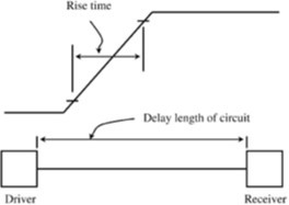
Rules of thumb states that “Terminate the transmission line in its characteristic impedance when the one-way propagation delay of the PCB track is equal to or greater than one-half the applied signal rise/fall time”’
Let’s take an example of Series and End terminations. The source termination method involves terminating the transmission line at its source, as depicted in below figure. This approach effectively absorbs the reflected waveform by employing an impedance matching that equals that of the transmission line. In this example, this requires about 39 Ω in series resistors with the internal output impedance of the driver, which is generally about 10 Ω. (ZO≈10Ω + Series termination resistance 39 Ω= Characteristics impedance of 50 Ω)
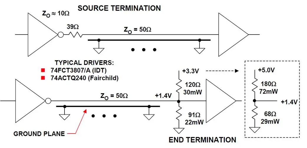
The end termination method, as illustrated in Figure, involves terminating the cable at its endpoint in the characteristic impedance of the Microstrip transmission line. Although higher impedances can be used, 50 Ω is popular because it minimizes the effects of the termination impedance mismatch due to the input capacitance of the terminating gate (usually 5 pF to 10 pF).
OFF Chip Terminations
In above example we can see these termination resistors are placed on PCB. When termination methods implemented external to an integrated circuit or chip than this type of implementations are called “OFF Chip Termination”.
On Die Terminations Features
- Terminating Input Signals: On-Die Termination (ODT) helps terminate input signals by matching the characteristic impedance of the transmission line. This is crucial for preventing signal reflections that can distort the transmitted data and degrade signal quality. By terminating the signal properly, the integrity of the communication can be maintained.
- Space Savings: On-die termination (ODT) is implemented directly on the integrated circuit (IC) die, eliminating the need for external discrete components such as resistors. This results in space savings on the circuit board.
- Cost Reduction: On-Die Termination (ODT) can contribute to cost reduction by eliminating the need for additional external components. This is particularly beneficial in high-volume manufacturing processes where cost efficiency is a key consideration.
- Receive Mode: On-Die Termination (ODT) is available in receive mode, where it helps terminate incoming signals to prevent reflections.
- Bidirectional Mode: In bidirectional mode, On-Die Termination (ODT) can be utilized for both input and output signals. This is especially relevant when the I/O (Input/Output) is bidirectional.
- In the context of memory interfaces like DDR (Double Data Rate) SDRAM (Synchronous Dynamic Random-Access Memory), On-Die Termination (ODT) is commonly used to match the transmission line impedance and optimize signal integrity during data transfer.
On-Die Terminations in DRAM
DRAM (DDR2/DDR3/DDR4/Next Gen DRAMs) technology possesses the capability to transfer data at significantly higher rates than previously achievable. Given these improved data rates, designers require options to enhance the signal integrity of the data bus while still preserving performance. The below pictures depict a DRAM I/O driver with On-Die Termination (ODT) capability, and simplified circuits are shown in the picture below for better understanding.
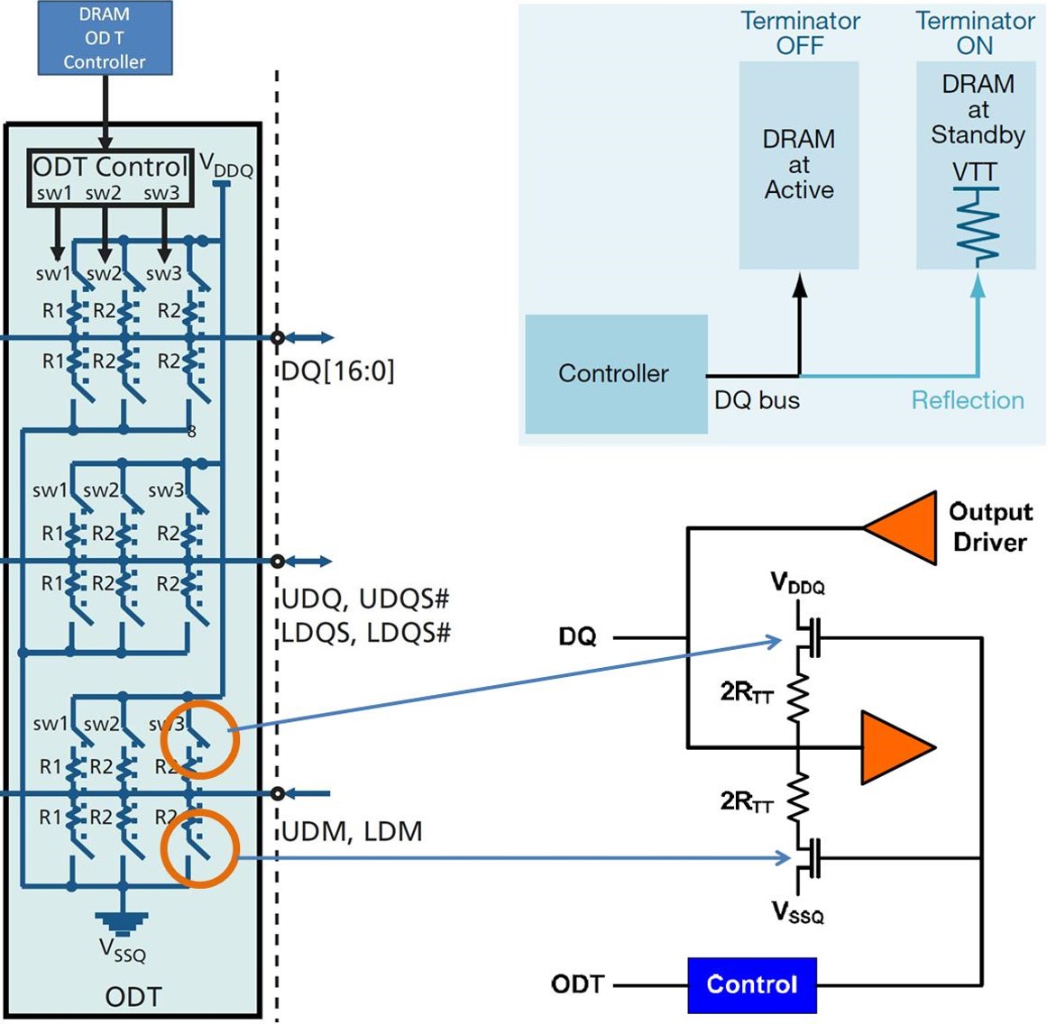
On-Die Termination (ODT) allows a DRAM to turn on/off termination resistance & related circuitry for each interface signal line as required (depending on the availability of the ODT feature on that specific signal/ device). This feature enhances the signal integrity of the memory channel by enabling the DRAM controller to independently turn on/off termination resistance for any or all DRAM devices.
How On-Die Termination (ODT) Works in DRAM?
Utilizing On-Die Termination (ODT) involves two steps. First, the On-Die Termination (ODT) value must be selected within the DRAM. Second, it can be dynamically enabled/disabled using the ODT pin from ODT Controller. To configure ODT ther could be different methods. FOR DRAM, it is done by setting up device’s extended mode register with proper ODT value.
There are synchronous and asynchronous timing requirements, depending on the state of the DRAM device. Essentially, the On-Die Termination (ODT) is turned on just before the data transfer and then shut off immediately after. If there is more than one DRAM device load on the channel, either the active or inactive DRAM can terminate the signal. This flexibility enables optimal termination to occur as precisely as needed.
DRAM Data Group Signals
Let’s us try to understand how On-Die Termination (ODT) works in DRAM Read write operations. All data-group signals fall under point-to-point singling. The data-group signals are driven by the DRAM controller on writes and driven by the DRAM memories during reads. No external resistors are needed on these routes on PCB as DRAM controller and Memory are equipped with ODT. The receivers in both cases (DRAMS memory on writes and DRAM controller on reads) will assert on-die terminations (ODT) at the appropriate times. The following diagrams show the impedances seen on these nets during write and read cycles.
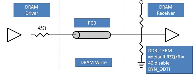
On-Die Termination (ODT) in Write Cycle
Let’s take an example that impedances seen on the nets during a write cycle as per below picture. During writes, the output impedance of the DRAM device is approximately 45Ω. It is recommended that the SDRAM be implemented with a 240Ω. Assuming RZQ resistor is 240Ω, Termination resistors can be configured to present an On-Die Termination (ODT) of RZQ/4 for an effective termination of 40Ω.
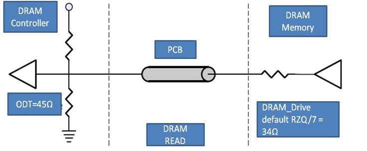
On-Die Termination (ODT) in Read Cycle
Below Picture shows the impedances seen on the PCB nets during a read cycle. During reads, it is recommended that the DRAM be configured for an effective drive impedance of RZQ/7 or 34 Ω (assuming RZQ resistor is 240 Ω). The on-die termination (ODT) within the DRAM controller will have an effective Thevenin impedance of 45 Ω.
Fly-By Signals
Now let’s talk about the fly-by signals, which include the address, control, command, and clock routing groups. The fly-by signals consist of the fly-by routing from the DRAM controller, stubs at each SDRAM, and terminations after the last SDRAM. In this example address, control, and command groups will be terminated through a 39.2-2 resistor to VTT.
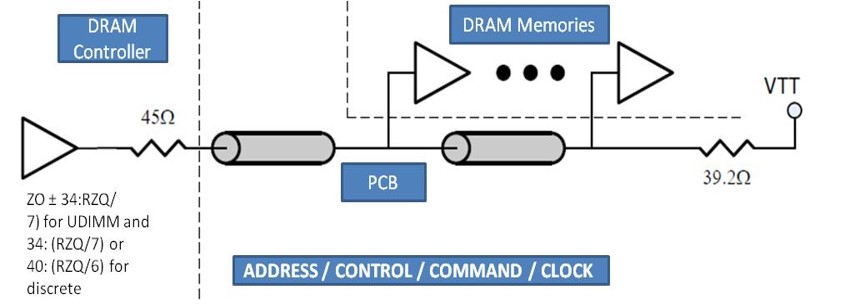
The clock pairs will be terminated through 39.2- resistors to a common node connected to a capacitor that is then connected to VDDQ. The DRAM controller will present a 45-2 output impedance when driving these signals.
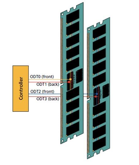
Two DIIM -Slot On-Die Termination (ODT) Routing
Below Figure shows the On-Die Termination (ODT) trace routing on a typical PC system with two memory slots. Each slot contains two ranks of memory (front and back). A separate ODT signal is routed to each rank of memory to provide flexibility in power management and the best system performance. The routing of ODT signals is like the routing of CS# signals.
On-Die Termination (ODT) in Write Cycle for DIIMs
Below Figure shows a typical termination scheme for write data in, one module (Left) and two-module (Right) system.
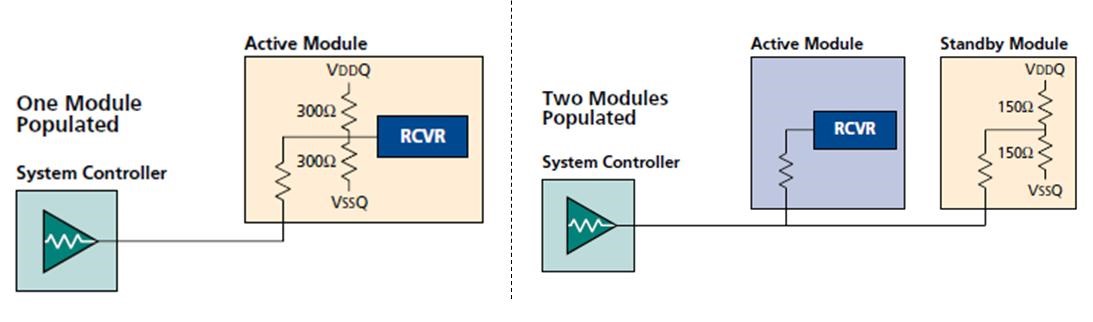
For example, If only one module is loaded in the system, a 150 ohm equivalent termination (300 ohm pul ohm pull-down) must be enabled on the module during the WRITE (above picture, Left).
If two modules are loaded into the system, the termination on the module not receiving the write data should be enabled at 75-ohm equivalent termination resistance (150 ohm pull-up/150 ohm pull-down). This termination scheme provides optimal trade-offs between signal integrity and voltage swing.
The equivalent comparison for write data at 533 Mbit/s is shown in below Figure.
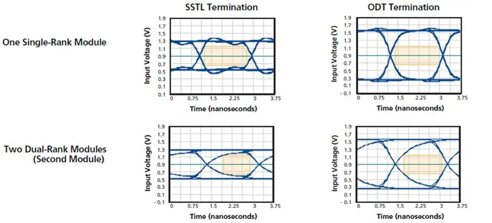
|
Parameters |
SSTL Termination (Left) |
ODT Termination(Right) |
|
Significant overshoot |
No |
No |
|
Voltage margin |
Outside the DRAM input voltage requirements |
Increased voltage margin |
|
Data Eye opening |
Comparatively Low |
Significantly larger, even under heavily loaded conditions |
On-Die Termination (ODT) in READ cycle for DIIMs
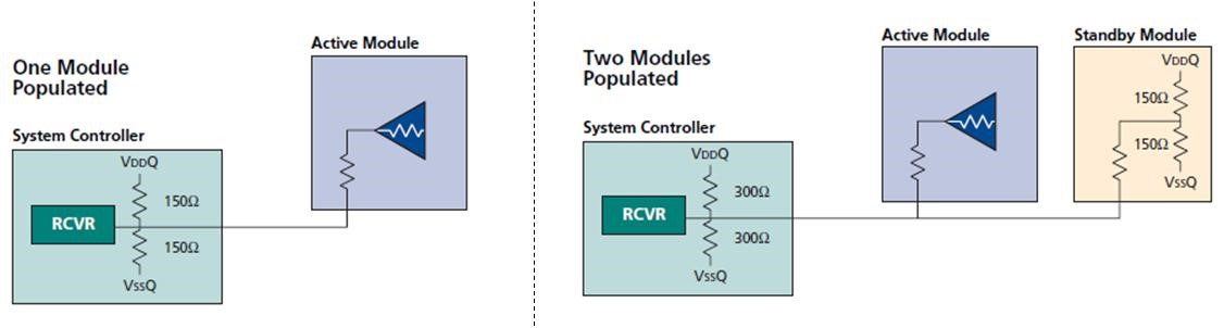
For READs, on-die termination must be included on the controller. For example if only one module is loaded in system, a 75 ohm termination should be enabled on the system controller. If two modules are loaded, the controller termination should be increased to 150 ohms and the unused module should terminate at 75 ohms. This configuration provides good voltage margin at the controller. Figure shows below a typical termination scheme for data in a 533 Mbit/s, two-module system.
Below picture shows a comparison of a DRAM(DDR2) DQ bus for a typical SSTL-terminated, module system using On-Die Termination (ODT) termination versus a non-ODT system reading data at 533 MTs.
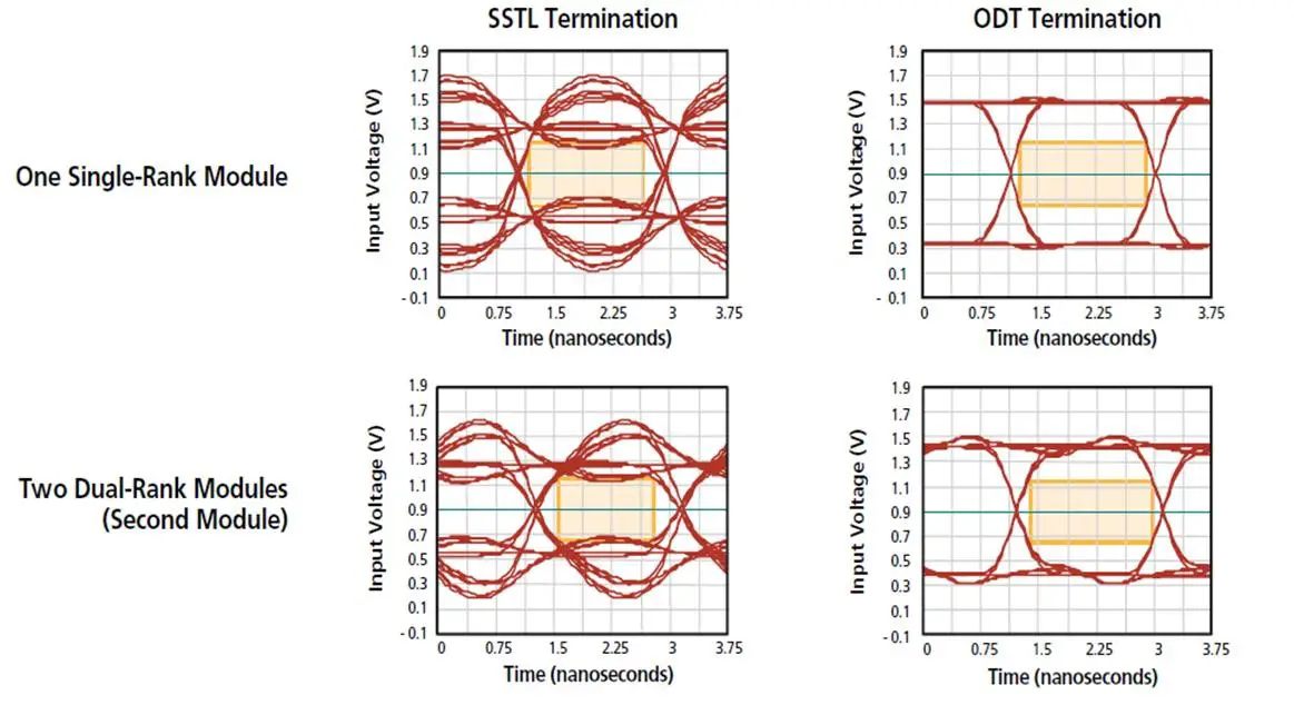
|
Parameters |
SSTL Termination (Left) |
ODT Termination(Right) |
|
Significant overshoot |
Yes |
No, overshoot reduction |
|
Voltage margin |
Poor |
Increased voltage margin |
|
Data Eye opening at higher load( Two DIIM) |
Starts “laying over” when more loads are added, which detracts from the timing margin |
Improvements dramatically & increase the size of the data eye |
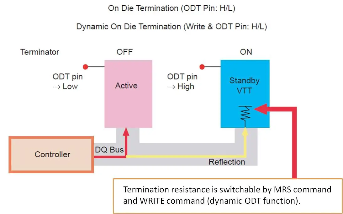
Dynamic On-Die Termination (ODT) (Dynamic On-Die Termination)
DRAM technology (3rd Generation and above) can transfer data at a much higher rate than previously possible. DRAM introduces a dynamic On-Die Termination (ODT) mode. In dynamic On-Die Termination (ODT), the impedance of the termination resistor can be dynamically varied in response to changes in data patterns, frequency, or temperature. This function allows dynamic switching of On-Die Termination (ODT) resistance during WRITE operations without the need for a Mode Register Set (MRS) command. Dynamic On-Die Termination (ODT) helps in optimizing termination under varying conditions, enhancing signal integrity and system performance.
Summary
Introduction to ODT
- Exploring “On-Die Terminations” requires understanding the concept of terminations.
- Electronic devices must meet expectations of high-speed data transfer, swift response, and real-time capabilities.
- Challenges arise with higher transfer speeds, reduced signal rise-fall times, and longer transmission lines, emphasizing the need for signal integrity.
Importance of Signal Integrity in High-Speed Digital Systems
- Signal integrity is crucial as data transfer rates increase over longer transmission media.
- It directly influences the performance, reliability, and efficiency of electronic devices.
- Refers to the signal’s quality as it passes through a transmission line, ensuring propagation without distortion.
- High-speed interconnections should be designed as transmission lines to minimize signal distortion, crosstalk, and electromagnetic radiation.
Introduction to Signal Termination
- Essential to terminate transmission lines at their characteristic impedance.
- Termination techniques minimize signal reflections, prevent data corruption, and ensure reliable communication.
- Critical in high-speed designs facing challenges like signal distortion, overshoot, and undershoot.
On-Die Terminations (ODT)
- Integrated into the IC, ODT helps terminate input signals, matching the transmission line’s characteristic impedance.
- Offers space savings on the circuit board by eliminating the need for external components like resistors.
- Contributes to cost reduction, available in receive and bidirectional modes.
- Commonly used in memory interfaces like DDR SDRAM to optimize signal integrity.
On-Die Terminations in DRAM
- DRAM technology, including DDR2/3/4 and next-gen DRAMs, transfers data at significantly higher rates and ODT helps them in improved SI.
- ODT allows dynamic control of termination resistance, enhancing signal integrity by preventing reflections.
- ODT improves voltage margin and data eye opening, reducing overshoot, and enhancing signal integrity compared to traditional SSTL termination.
Dynamic ODT
- Modern DRAM technology introduces dynamic ODT, allowing dynamic variation of termination resistance.
- No need for a Mode Register Set command.
- Optimizes termination under varying data patterns, frequencies, or temperatures.
- Enhances overall signal integrity and system performance.
Author Profile
- 20+ years embedded hardware design professional with a burning passion for teaching. Sharing the intricate world of embedded hardware is my mission and joy.
Latest entries
 Tech Updates30 November 2025STM32WBA6: The Next-Generation MCU Powering Secure Short-Range Wireless Designs
 Blogs24 November 2025High-Speed PCB Layout Design Guide-104
 Tech Updates14 September 2025Renesas Launches RL78/L23 Ultra-Low-Power MCUs to Power Smarter Home Appliances
 Blogs7 September 2025High-Speed PCB Layout Design Guide-103