The interface of DDR SDRAM (Double Data Rate Synchronous Dynamic Random Access Memory) provides higher transfer rates than single data rate (SDR) SDRAM by allowing data transfers on both the rising and falling edges of the clock cycle, effectively doubling the transfer rate. DDR SDRAM offers various advantages, including faster data transfer rates, increased bandwidth, improved power efficiency, higher capacity, and synchronization with the system clock(Source Synchronous).
DDR SDRAM implementations often incorporate technologies such as phase-locked loops and self-calibration to achieve the required timing accuracy for these benefits. This makes DDR SDRAM a more efficient and high-performance choice for modern memory systems compared to SDR SDRAM.
DDR SDRAM Memory Signal Definition
|
Signal Name |
Descriptions |
Active Level |
Directions(From SDRAM Controller to Memory) |
|
CK/nCK |
Differential System Clock |
On rising/Falling edge |
Output |
|
CKE |
SDRAM Clock Enable |
High |
Output |
|
CS |
SDRAM Controller Chip Select |
Low |
Output |
|
BA[1:0] |
Bank Select Signals |
NA |
Output |
|
RAS |
Row Signal |
Low |
Output |
|
CAS |
Column Signal |
Low |
Output |
|
WE |
SDRAM Write Enable |
Low |
Output |
|
D[31:0] |
Data Bus |
NA |
Bidirectional |
|
A[12:0] |
Address Bus |
NA |
Output |
|
DQMLDM, UDM |
Data Mask |
On rising/Falling edge |
Output |
|
UDQS, LDQS |
Data Strobe |
NA |
Bidirectional |
|
VDD |
Power supply (for the internal circuit) |
NA |
Power |
|
VSS |
Ground (for the intimae circuit) |
NA |
Power |
|
VDDQ |
DQ power supply |
NA |
Power |
|
VREF |
Referential voltage |
NA |
Power |
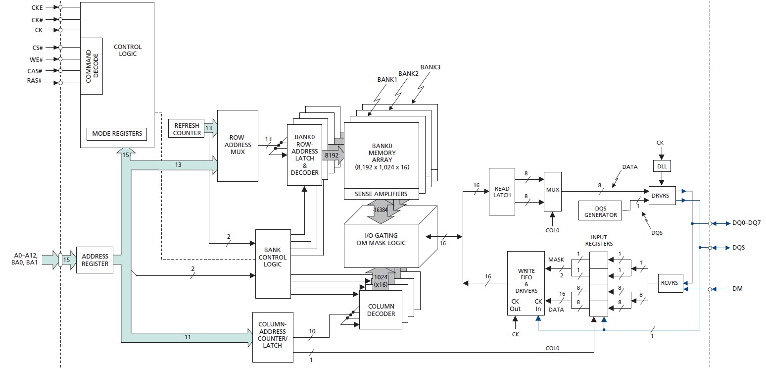
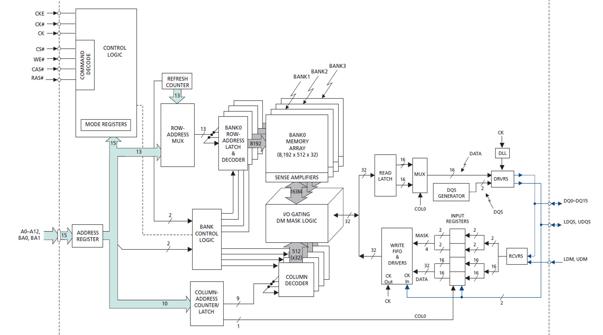
DDR SDRAM Memory Interface
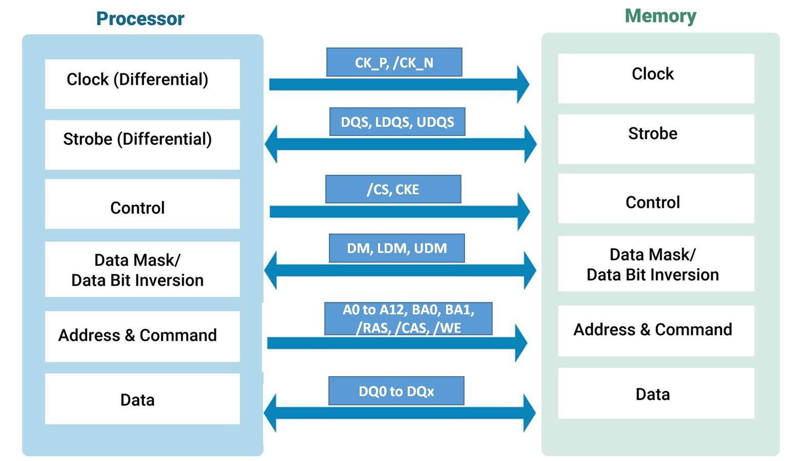
DDR SDRAM devices use several signals for control and data transfer. Few of the key DDR SDRAM is as below:-
CK, nCK(System Clock)
DDR SDRAM differential Clock, samples data on rising/falling edge. This is the primary clock signal from the DDR SDRAM controller to memory that controls the timing and synchronizes the operation of all DDR SDRAM operations. All input signals except data input/output (DQ), DQ write mask enable (DM), and data strobe (DQS), are sampled on the rising/falling edge of this clock signal.
CKE
DDR SDRAM Clock Enable. CKE acts as an inhibit signal for DDR SDRAM. The CKE determines whether the clock (CK) is valid or invalid. If the Clock Enable (CKE) signal is high at the rising edge of the clock (CK), the next rising edge is valid, allowing operations to proceed. If CKE is not high at the rising edge, the next rising edge is invalid, preventing associated operations. When CKE goes low, it signifies that the DDR SDRAM device is entering a power-down mode. Like power-down mode, CKE is driven low, when the DDR SDRAM devices to be kept in ideal and self-refresh mode by issuing the self refresh command.
CS (Chip Select)
The Chip Select signal is used to enable (sampled LOW) or disable (sampled 1GH) the SDRAM device. When active (typically low), command input is valid & DDR SDRAM responds to commands and data. When the CS signal is high, all commands are ignored but the operation continues.
DQ [31:0] (Data In/Out)
The DQ input/output Data Bus signals for reading from and writing to the memory are synchronized with the positive and negative edges of CLK. The IOs are byte-makeable during Reads and Writes
A(n:0)- Address bus
A(n:0) are sampled during the ACTIVE command and READ/WRITE command with A10 defining auto precharge to select one location out of the memory array in the respective bank. The number of address lines than need to be sampled depends upon memory configurations 4-Bits, 8-Bits, 16-Bits, or 32-Bits, with which memory is interfaced with a processor. A10 is sampled during a PRECHARGE command to determine whether all banks are to be recharged (A10 HIGH) or the bank selected by BA (1.0) [A1 LOW).
DOM (Data Mask)
Data Mask signals are issued by DDR SDRAM controller to the memory, sampled during a write cycle and are used to mask data bytes and allow selective writing specific bytes or words within a larger data width. For memory, it is an input mask signal for write accesses and an output enable signal for read accesses. For example, 32-bit SDRAM will have DOM (3:0). DQM3 masks DQ31-0024 DQM2 masks DQ23-0016, DQM1 masks DQ15-DQ8, and DQM0 masks DQ7-DQ0.
Data strobe signal (DQS)
DDR SDRAM, Similarly to SDR SDRAM, is controlled by command input signals synchronized with the rising edge of the clock (CK). However, its data input/output timing differs, as DDR SDRAM transfers data on both the rising and falling edges of the clock signal, effectively doubling the data transfer rate compared to SDR SDRAM. To achieve high-speed data transfer, DDR SDRAM introduces a data strobe signal called DQS, which is output from memory controller to DDR SDRAM.
This DQS signal is essential for adjusting the data capture timing at the receiver end, ensuring accurate sampling of data (DQ) even at higher clock speeds. The receiver utilizes the DQS signal to fine-tune the timing for capturing the data, thereby enhancing data integrity and reliability in the process. In summary, DDR SDRAM employs a combination of dual-edge data transfer and the use of a data strobe signal (DQS) to achieve faster data transfer rates while maintaining precise data capture timing.
CAS (Column Address Strobe)
The Column Address Strobe CAS# is an active low command signal issued by the DDR SDRAM controller to DDR SDRAM Memory. It is issued within conjunction with the RAS# and signals and is latched at the positive edges of CLK. Different signal levels of RAS, CAS. WE and CS SDRAM controller issues different types of commands to SDRAM to perform different operations.
For example, when RAS is held “HIGH” and CS# is asserted “LOW,” the column access is started by asserting CAS# “LOW.” Then, the Read or Write command is selected by asserting WE# “LOW” or “HIGH”.
RAS (Row Address Strobe)
The row address strobe RAS# is an active low command signal issued by DDR SDRAM controller to DDR SDRAM Memory. It is issued in conjunction with the CAS# and WE signals and is latched at the positive edges of CLK. Different signal levels of RAS, CAS. WE and CS SDRAM controller issues different type of commends to SDRAM to perform different operations.
For Example, When RAS# and CS# are asserted “LOW and CAS is asserted “HIGH” either the BankActivate command or the Precharge command is selected by the WE signal When the WEB is asserted “HIGH,” the BankActivate command is selected and the bank designated by BA is turned on to the active state. When the WEP isasserted “LOW,” the Precharge command is selected and the bank designated by BA is switched to the idle state after the precharge operation.
WE (Write Enable)
The Write Enable signal WE is an active low command signal issued by DDR SDRAM controller to DDR SDRAM Memory. It is issued in conjunction with RAS and CAS signals and is latched at the positive edges of CLX. The WEB input is used to select the BankActivate or Precharge command and Read or Write command.
BAn (Bank Address)
The Bank Address issued by DDR SDRAM controller to DDR SDRAM Memory. These signals specify which bank within the DDR SDRAM is being accessed Multiple banks are common in SDR SDRAM devices, and these signals select the appropriate bank. For example two signals BAO, BA1 can select 4 banks by 4 differentlogic level combinations possibility on these signals.
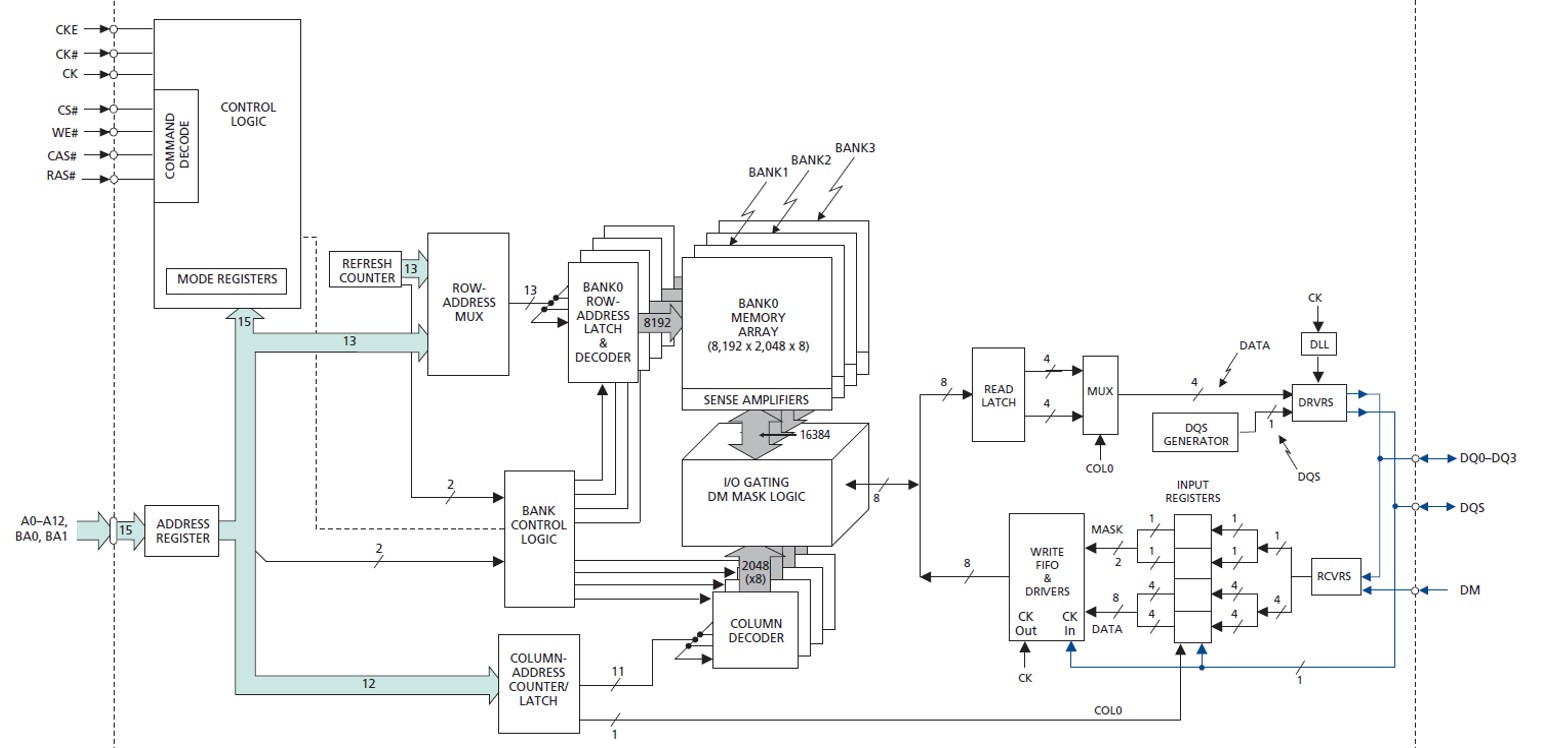
SDRAM Read/Write Operations
In DDR SDRAM, the memory access process involves loading a bank address and a row address with an active command, selecting the corresponding word line. Subsequently, a bank address and a column address are loaded with a read or write command, selecting the corresponding digit line. The DDR SDRAM incorporates a Delay Locked Loop (DLL) circuit designed to minimize timing skew between external and internal clock signals, enabling fast access and high operation frequencies. The DLL controls and adjusts the time lag, ensuring synchronization. With this architecture, 2n bits of data are transferred from the memory cell array to the I/O buffer every clock cycle. The output occurs in n-bit segments (even and odd addresses) every half-clock cycle, resulting in continuous data output synchronized with both the rising and falling edges of the clock. This design enhances the efficiency and speed of data transfer in DDR SDRAM.
In a DDR SDRAM read operation, the sequence is as follows:
- Activate a specific row in a particular bank by issuing the bank active command (ACT) along with a row address and bank address.
- After a time interval of tRCD from the ACT command, provide the starting column and bank addresses with the READ command.
- After a time interval of /CAS latency from the READ command, the read burst data becomes available, starting from the specified column address in step 2. The number of successive burst data is determined by the burst length (BL).
- After a time interval of tRAS from the ACT command, input the precharge command (PRE). To output all burst data, the earliest timing for the PRE command is (burst length/2) clocks after the READ command.
In DDR SDRAM, a write operation follows this sequence:
Activate a specific row in a particular bank by issuing the bank active command (ACT) along with a row address and bank address.
- After a time interval of tRCD from the ACT command, provide the starting column and bank addresses with the WRIT command.
- During write bursts, the first valid data-in element is registered on the first rising edge of the data strobe signal (DQS), and subsequent data elements are registered on successive edges of DQS.
- After a time interval of tRAS from the ACT command, input the precharge command (PRE).
- After a time interval of tRP, the corresponding bank becomes idle.
SDRAM Addressing
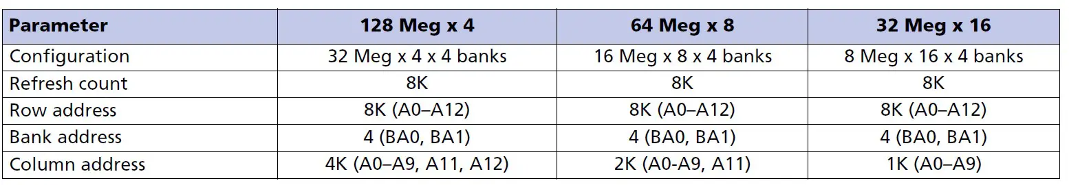
Functional Block Diagram:- 128 Meg Locations x 4-Bits Bus
Memory calculations for above memory DDR SDRAM organizations: –
Data Bus Width = 4-Bits
No of Row Address Bits: – 13
No of Column Address Bits: – 12
No of Banks = 4
Total number of Memory locations in the DDR SDRAM=
2^No of Row Address Bits x 2^ No of Column Address Bits x No of Banks
= 2^13 x 2^ 12 x 4 = 2^13 x 2^ 12 x 2^2 = 2^27 =128 Mega locations
Total Size of DDR SDRAM memory =
Data Bus Width x Total number of Memory locations in the DDR SDRAM
= 4- bit x 128 Mega locations = 512 Mega Bits
Functional Block Diagram:- 32 Meg Locations x 8-Bits Bus
Memory calculations for above memory DDR SDRAM organizations:-
Data Bus Width = 8-Bits
No of Row Address Bits: – 13
No of Column Address Bits: – 11
No of Banks = 4
Total number of Memory locations in the DDR SDRAM=
2^No of Row Address Bits x 2^ No of Column Address Bits x No of Banks
= 2^13 x 2^ 11 x 4 = 2^13 x 2^ 11 x 2^2 = 2^26 = 64 Mega locations
Total Size of DDR SDRAM memory =
Data Bus Width x Total number of Memory locations in the DDR SDRAM
= 8-Bits x 64 Mega locations = 512 Mega Bits
Functional Block Diagram:- 32 Meg Locations x 16-Bits Bus
Memory calculations for above memory DDR SDRAM organizations: –
Data Bus Width = 16-Bits
No of Row Address Bits: – 13
No of Column Address Bits: – 10
No of Banks = 4
Total number of Memory locations in the DDR SDRAM=
2^No of Row Address Bits x 2^ No of Column Address Bits x No of Banks
= 2^13 x 2^ 10 x 4 = 2^13 x 2^910 x 2^2 = 2^25 = 32 Mega locations
Total Size of DDR SDRAM memory =
Data Bus Width x Total number of Memory locations in the DDR SDRAM
= 16-Bits x 32 Mega locations = 512 Mega Bits
Summary
To interface DDR SDRAM memory, you need to understand the key signals and commands involved in the DDR SDRAM interface. Here’s a summarized guide:
Key DDR SDRAM Signals:
- CK/nCK (System Clock):
- Differential clock that samples data on rising/falling edges.
- Primary clock signal controlling timing and synchronization.
- CKE (Clock Enable):
- Inhibits or allows the clock (CK) to be valid.
- Determines if the next rising edge is valid for operations.
- CS (Chip Select):
- Enables or disables the SDRAM device.
- Active (low) when commands are valid; inactive when CS is high.
- DQ [31:0] (Data Bus):
- Bidirectional data bus for reading from and writing to memory.
- A[12:0] (Address Bus):
- Output address bus sampled during commands to select memory locations.
- DQM (Data Mask) and DQS (Data Strobe):
- DQM masks data bytes during writes.
- DQS helps adjust data capture timing for precise sampling.
- RAS (Row Address Strobe) and CAS (Column Address Strobe):
- Control row and column access, respectively, during memory operations.
- WE (Write Enable):
- Activates write operation when low during the proper command sequence.
- BA[1:0] (Bank Select):
- Selects one location out of the memory array in the respective bank.
DDR SDRAM Commands:
- ACT (Activate): – Activates a specific row in a bank.
- READ and WRITE: – Reads or writes data after a specific row is activated.
- PRE (Precharge):-Returns the bank to the idle state after a read or write operation.
- MRS and EMRS (Mode Register Set):- Configures mode registers, only when all banks are in the idle state.
- REF (Refresh):- Initiates auto-refresh to maintain memory integrity.
DDR SDRAM Operation Sequence:
Read Operation:
- ACT command to activate a specific row.
- READ command to read data from the activated row.
- PRE command to precharge the bank after reading.
Write Operation:
- ACT command to activate a specific row.
- WRITE command to write data to the activated row.
- PRE command to precharge the bank after writing.
SDRAM Addressing:
- DDR SDRAM uses a combination of row and column addresses to access memory locations.
- The number of row and column address bits depends on the specific DDR SDRAM organization (e.g., 13 row bits, 12 column bits).
Truth Table – Commands:
- DDR SDRAM operates through various command states like IDLE, BANK ACTIVE, READ, WRITE, etc.
- Each state has specific conditions and transitions.
- Understanding these signals, commands, and operations is crucial for effectively interfacing with DDR SDRAM memory in a system.
DDR SDRAM Read/Write Operations:
- Read operation involves activating a row, providing column and bank addresses, and reading burst data.
- Write operation involves activating a row, providing column and bank addresses, writing burst data using the data strobe signal (DQS), and precharging.
SDRAM Addressing:
- Addressing involves row and column address bits, with the number of banks determining the total number of memory locations.
- Memory calculations are based on the data bus width, row address bits, column address bits, and the number of banks.
Memory Calculations:
- Examples provided for DDR SDRAM organizations with different data bus widths (4-Bits, 8-Bits, 16-Bits).
- Calculations include determining the total number of memory locations and the total size of DDR SDRAM memory.
Functional Block Diagrams:
- Functional block diagrams illustrate DDR SDRAM organizations with different configurations.
- Configurations include data bus width, row address bits, column address bits, number of banks, total memory locations, and total memory size.
Author Profile
- 20+ years embedded hardware design professional with a burning passion for teaching. Sharing the intricate world of embedded hardware is my mission and joy.
Latest entries
 Tech Updates30 November 2025STM32WBA6: The Next-Generation MCU Powering Secure Short-Range Wireless Designs
 Blogs24 November 2025High-Speed PCB Layout Design Guide-104
 Tech Updates14 September 2025Renesas Launches RL78/L23 Ultra-Low-Power MCUs to Power Smarter Home Appliances
 Blogs7 September 2025High-Speed PCB Layout Design Guide-103