RS-485 is a balanced data transmission standard for serial communication. RS-485 facilitates the robust transmission of moderate data rates across long distances in multipoint communication applications. It finds extensive use in applications such as factory and building automation, motor control, and other field bus applications.
RS485 formally known as American National Standards Institute (ANSI) Telecommunications Industry Association (TIA)/Electronic Industries Alliance (EIA)-485-A.
Numerous advanced interface standards, including the Modicon bus (ModBus), process field bus (ProfiBus), DMX512, and others, rely on RS-485 as their physical layer.
Also Read : What is Ethernet
Key Features and Specifications of RS485 Communication
Key features of RS-485 are:
- Balanced interface: RS-485 uses a balanced transmission line, meaning it has two signal wires carrying equal and opposite signals to reduce noise and improve signal integrity.
- Multiple Drivers, Multiple Receivers: RS-485 standard supports multiple drivers and receivers on the same communication bus. This allows for the creation of multipoint networks where several devices can communicate over the same twisted-pair cable.
- Half-Duplex: RS-485 typically operates in half-duplex mode, meaning data can be transmitted and received, but not simultaneously. On the other hand, RS-422 commonly supports full-duplex operation, allowing for simultaneous transmission and reception of data.
- Multipoint operation from a single 5-V or 3.3V supply: RS-485 allows multiple devices (up to 32 unit loads) to be connected to the same communication bus, powered by a single 5-volt or 3.3-volt power supply.
- –7-V to +12-V bus common-mode range: This indicates the range of voltages that the RS-485 bus can tolerate without affecting communication reliability. It means the difference between the voltages on the two signal wires can range from -7 volts to +12 volts.
- Up to 32 unit loads
- 10-Mbps maximum data rate (at 40 feet)
- 4000-foot maximum cable length (at 100 kbps)
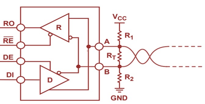
Functional Block Diagram of RS485 Transceiver
An RS-485 transceiver typically integrates several key components into a single chip to facilitate reliable communication over RS-485 networks. Those components are driver, receiver, and circuitry for ESD and bus fault protection.
Below figure shows the typical functional block diagram of RS485 Transceiver:
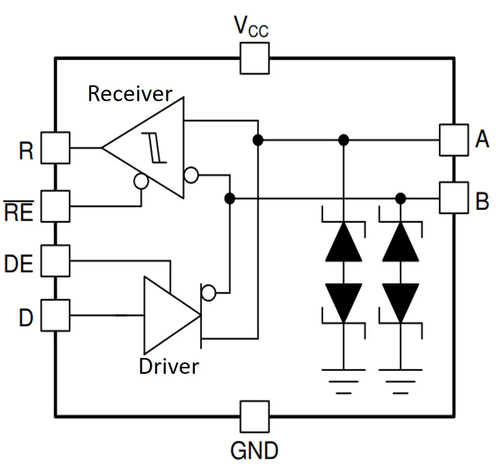
Pinout Description of an RS485 Transceiver
|
Pin Name |
Description |
|
VCC |
Bus Supply (3.3V or 5V) |
|
GND |
Local Device Ground |
|
A |
RS485 Bus A |
|
B |
RS485 Bus B |
|
R |
Receive data output (Digital Output) |
| RE |
Receiver enable input (Digital Input) |
|
DE |
Driver enable input; integrated pull-down (Digital Input) |
|
D |
Transmission data input (Digital Input) |
Network Topology of RS485 Communication Protocol
In RS-485 networks, multiple nodes are interconnected in parallel to form a bus, known as the bus topology. The drivers and receivers, called as transceivers link to a primary cable trunk through short network stubs in this arrangement.
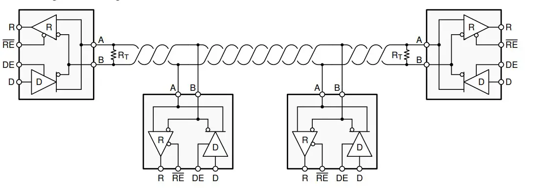
The above figure shows the typical network connections for half-duplex (two-wire) RS-485 implementations.
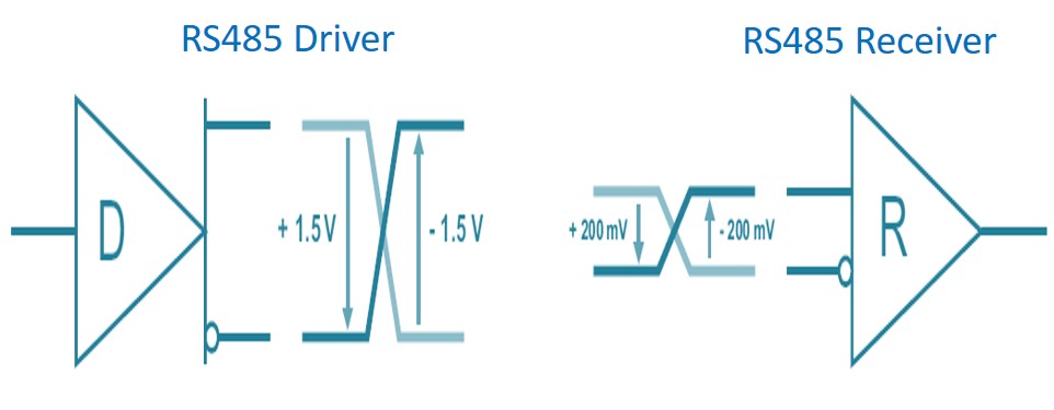
RS485 Transceiver Voltage Levels
RS-485 compliant drivers deliver a minimum differential output of 1.5 V over a 60-Ω load, while compliant receivers can detect a minimum differential input of 200 mV. These specifications offer a considerable margin, ensuring dependable data transmission even in the face of significant signal degradation across cables and connectors. This robustness is the main reason why RS-485 is well-suited for long-distance networking in noisy environments.
The RS485 Driver
The provided diagram illustrates the equivalent output schematic of the RS485 driver. It demonstrates that the driver’s fundamental operation can be understood in terms of its high- and low-output logic states. The output configuration incorporates an H-bridge driver featuring high- and low-side transistors for both the A and B outputs.
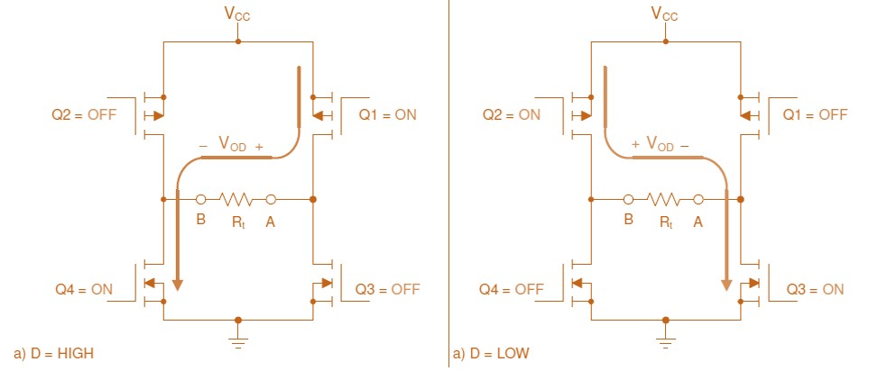
The resulting waveform can be described as a positive and negative differential voltage superimposed on a common-mode offset voltage, typically close to VCC/2.
According to the RS-485 standard, an RS485-compliant driver is required to deliver a differential output voltage greater than 1.5 V when driving a 60-Ω load, as well as a common-mode load of 375 Ω from both the A and B outputs, within the range of -7 V to 12 V.
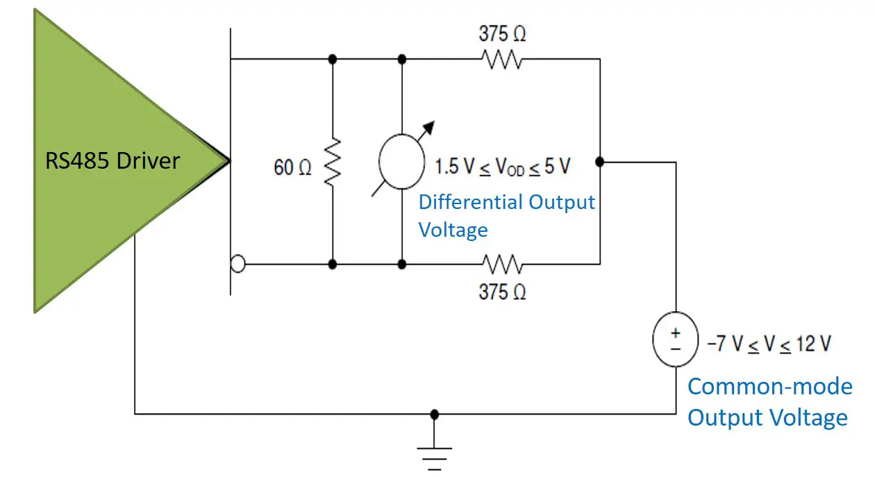
RS-485 stands out from other signaling standards due to its significant differential output voltage and extensive common-mode range. These characteristics make it well-suited for operation in noisy electrical environments and various applications, including industrial automation, e-metering, and motor control.
The RS485 Receiver
The receiver input circuit includes electro-static discharge (ESD) protection, a resistor-divider network, and biasing current, influencing the magnitude and common-mode voltage reaching the differential comparator. For half-duplex transceivers, both the driver and receiver utilize shared ESD protection.
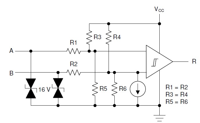
There are two functions of the resistor-divider network present on the A and B inputs of the comparator.
The first function is to attenuate large signals that are beyond the range of the supply voltage of the receiver. As per RS-485 standard the common mode must be in between –7 V to +12 V on the bus terminals and that exists between transceivers on a shared network.
These high voltages need attenuation down to voltages that 3.3 V or 5 V transceivers can handle. A typical attenuation factor should be on the order of 10 to 1, effectively reducing the magnitude of the voltages present internally at the comparator.
The second important function of the resistor-divider network is to bias the bus voltages toward VCC/2. This is necessary because simply attenuating a negative signal will not bring the voltage between the local ground of the receiver and VCC. Attenuating the signal and biasing it toward VCC/2 prevents the inputs of the comparator from getting saturated; thus enabling the comparator to properly evaluate the differential voltage between the A and B terminals.
In the above figure, there is a current source connected between the B input terminal of the comparator and the ground. the current source will cause a voltage drop across
R4 and R6 are connected to the negative input terminal of the comparator. This creates a fail-safe bias voltage that causes the negative terminal to have a lower voltage than the positive terminal and the output of the comparator to be in a known high state when applying a 0-V differential voltage to the A and B pins. This fail-safe biasing helps ensure that the Receiver output will be high in the presence of bus idle or bus short-circuit conditions.
Differential Input Threshold Voltage of an RS485 Receiver
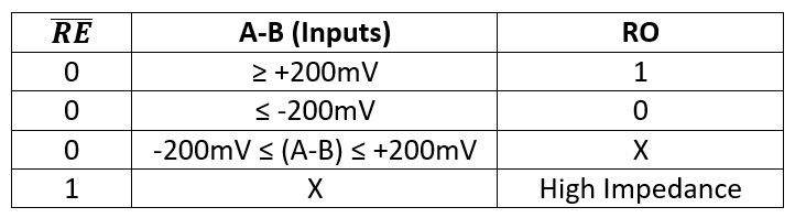
The differential input threshold voltage (VTH) of a receiver refers to the voltage level on the receiver input that ensures a transition (from low to high or high to low) of the receiver output. Typically, an RS-485 transceiver has a differential input threshold voltage of ±200 mV. This indicates that when the differential input equals or exceeds 200 mV (VIA – VIB ≥ 200 mV), the receiver output is assured to be high (RO = 1). Conversely, when the differential input is equal to or less than -200 mV (VIA – VIB ≤ -200 mV), the receiver output is guaranteed to be low (RO = 0). Refer to the truth table below for the receiver’s behavior.
Fail-Safe Biasing in RS485 Network
RS-485 operates on a multipoint topology network and cannot manage contention. This means that at certain times, all RS-485 transceivers on the bus may present a high impedance state, resulting in no actively driven logical state. Typically, this occurs between the transmission of messages by different nodes. During such periods, the bus may exhibit a 0-V differential signal due to the presence of a termination resistor.
To address this indeterminate state, two common methods are employed. One method involves selecting receivers with built-in fail-safe input thresholds. Another approach is to use additional external resistors to establish an external bias on the idle bus. Both methods ensure that the bus maintains a logical high state, corresponding to a positive differential voltage.
In the built-in fail-safe input bias method, (explained in the previous section) extra circuitry incorporates large pull-up and pull-down resistors on the receiver inputs. These resistors, typically around 100 kΩ, form a potential divider with line-termination resistors, generating only a few millivolts differentially. Although this voltage may be insufficient to switch the receiver state directly, an internal bias current within the attenuation network creates a voltage difference at the receiver comparator input.
One advantage of this solution is that it doesn’t impact the loading of transceivers on the network. However, a drawback is that every node on the network must feature this built-in capability. For existing installations or setups with previously designed modules that are challenging to update, implementing this method may not be feasible.
Another approach to managing idle bus conditions involves using two external resistors: one connected from the A terminal to VCC and the other from the B terminal to the ground. These resistors, depicted in the figure below, are common circuits utilized to provide an external hard-wired failsafe for an RS485 network.
The objective of each circuit is to uphold a voltage at the receiver inputs above the minimum input threshold and ensure a known logic state under one or more of three fault conditions. In the provided circuit, RT represents the resistors used for impedance matching of the transmission line, and they contribute to a voltage divider setup that establishes the steady-state bias voltage.
![\[ \ R_1 = R_2 = R} \]](https://embeddedhardwaredesign.com/wp-content/ql-cache/quicklatex.com-8de88d84c174a11cb3259d67cb427282_l3.png "Rendered by QuickLaTeX.com")
![\[ \ V_A - V_B \geq 200 \, \text{mV} \]](https://embeddedhardwaredesign.com/wp-content/ql-cache/quicklatex.com-7a3f57727a9a9fcf6435e937afbda75a_l3.png "Rendered by QuickLaTeX.com")
![\[ V_A - V_B = R_T \left( \frac{V_{\text{CC}}}{2R + R_T} \right) = 200 \, \text{mV} \]](https://embeddedhardwaredesign.com/wp-content/ql-cache/quicklatex.com-9ef400d2a0e447c1ef1cb607cbfd145d_l3.png "Rendered by QuickLaTeX.com")
If  , then
  . If
. If  , then
  .
.
Termination in RS485 Bus, and How to Do It Properly
Transmission lines should always be properly terminated, with short stubs, to prevent signal reflections. Effective termination involves matching the terminating resistors, RT to the characteristic impedance, Z0 of the transmission cable.
The standard 120-Ω value for termination resistors corresponds to the differential-mode characteristic impedance of the twisted-pair bus wires. This impedance is determined by factors such as wire gauge, insulation type and thickness, and the number of twists per unit length, which collectively influence the impedance detected by high-speed data signals. Typically ranging from 100 Ω to 150 Ω for twisted-pair cables, the RS-485 standard writers chose 120 Ω as the nominal characteristic impedance, aligning termination resistors with this value.
Matching the cabling’s characteristic impedance to the termination network allows the receiver to maximize signal power detection. Failure to terminate the transmission line properly, or terminating with a value different from the cable’s impedance, introduces mismatches that cause reflections at the network ends. Reflections occur when some signal energy returns up the line, potentially interfering constructively or destructively with subsequent bits propagating down the bus.
In applications where the bit time closely aligns with the cable loop time, termination is vital to minimize reflections. Basic termination networks, such as standard parallel termination networks, typically employ a single resistor.
However, termination networks may not be necessary when the two-way loop time of the network significantly exceeds a single bit time (approximately < 0.1 × two-way loop delay). In such cases, reflections lose energy with each trip to the end of the network.

Unit Loads and the Maximum Number of Nodes on the RS485 Network
RS-485 functions as a multipoint differential bus, meaning that all nodes on the bus share a single transmission medium. Consequently, each added node imposes a load in parallel on all existing network transceivers and termination resistors. As the total number of nodes increases, so does the loading on each driver.
Unit Load (UL) in RS485 Bus
To establish practical and measurable limits for RS-485 output drivers, the TIA/EIA-485 standard introduced the concept of a “unit load” and restricted the maximum number of unit loads any driver on an RS-485 bus can handle to 32. This standard mandates that a driver must maintain a minimum 1.5 differential signal across a maximum of 32 unit loads, in addition to two 120-Ω termination resistors.
The unit load can be determined as per the below formula considering the unit-load parameter by sweeping the input voltage (Vin) from –7 to 12 V on one bus pin, with the other bus pin held at the ground.
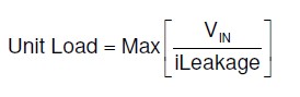
One-unit load (UL) is equivalent to 1 mA of input leakage current at 12 V. This load represents a single-ended load concerning the ground. Another easy way to think of the unit load is the equivalent of a 12-kΩ resistance from either the A or B bus pins to the ground.
Number of Nodes on RS485 Bus
Modern transceivers often offer reduced unit loading, such as 1/8 UL, enabling the connection of up to 256 transceivers on the bus. However, failsafe biasing contributes up to 20 unit loads of bus loading, thus reducing the maximum number of transceivers, denoted as N
![\[ N = \frac{32 \, \text{UL} - 20 \, \text{UL Due to FailSafe}}{\text{UL\_per\_transceiver}} \]](https://embeddedhardwaredesign.com/wp-content/ql-cache/quicklatex.com-2f52c71d50a770673880a897e6dff4b3_l3.png "Rendered by QuickLaTeX.com")
Thus, when using 1/8-UL transceivers, it is possible to connect up to a maximum of 96 devices to the bus.
|
Unit Load |
Bus Leakage Current at 12 V |
Equivalent Input Resistance |
Maximum Nodes on One Network |
Maximum Nodes on One Network considering fail-safe biasing |
|
1 |
1 mA |
12 kΩ |
32 |
12 |
|
1/2 |
500 μA |
24 kΩ |
64 |
24 |
|
1/4 |
250 μA |
48 kΩ |
128 |
48 |
|
1/8 |
125 μA |
96 kΩ |
256 |
96 |
Stub Length of RS485
The electrical length of a stub, (the distance between a transceiver and cable trunk), should be shorter than 1/10 of the driver’s output rise time, and is given through:
![\[ \text{Stub Length (L in feet)} \leq \frac{tr \times v \times c}{10} \]](https://embeddedhardwaredesign.com/wp-content/ql-cache/quicklatex.com-5d6f106dffcbf26b006d705eb7388338_l3.png "Rendered by QuickLaTeX.com")
Where
tr = Driver Rise time
v= Signal velocity of the cable
c = Speed of light in feet per second
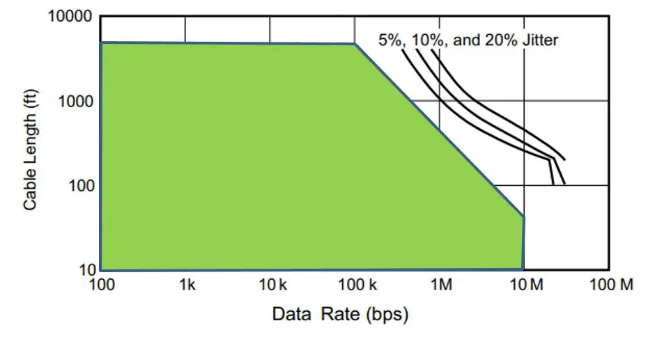
Data Rate and Bus Length
An inverse relationship exists between data rate and cable length in RS-485 systems. This implies that higher data rates correspond to shorter cable lengths, while lower data rates allow for longer cable lengths. Although the majority of RS-485 systems operate within the range of 10 kbps to 100 kbps, certain applications demand data rates of up to 250 kbps over distances exceeding 4000 feet. Achieving longer distances often involves accepting small signal jitter, typically up to 5 or 10%.
Author Profile
- 20+ years embedded hardware design professional with a burning passion for teaching. Sharing the intricate world of embedded hardware is my mission and joy.
Latest entries
 Tech Updates30 November 2025STM32WBA6: The Next-Generation MCU Powering Secure Short-Range Wireless Designs
 Blogs24 November 2025High-Speed PCB Layout Design Guide-104
 Tech Updates14 September 2025Renesas Launches RL78/L23 Ultra-Low-Power MCUs to Power Smarter Home Appliances
 Blogs7 September 2025High-Speed PCB Layout Design Guide-103