The Media-Independent Interface (MII) serves as a standardized method for connecting Ethernet MAC (Media Access Control) devices to PHY (Physical Layer) devices. Its primary purpose is to facilitate communication between these two essential components of an Ethernet system.
Media-Independent Interface (MII)
The Media-Independent Interface (MII) is a parallel interface defined by the IEEE 802.3 standard. The management interface of the MII allows the configuration and control of multiple PHY devices, the gathering of status and error information, and the determination of the type and abilities of the attached PHY(s). It establishes the communication protocol and electrical signaling between the MAC(which manages data transmission) and the PHY (which handles the physical transmission medium, such as copper or fiber optics).
Features of Media-Independent Interface (MII)
- Interoperability: Media-Independent Interface (MII) enables interoperability between different manufacturers’ MAC and PHY devices. Standardization ensures that MACs from one vendor can communicate seamlessly with PHYs from another, promoting compatibility and flexibility in network design.
- Data Transmission: Media-Independent Interface (MII) facilitates the transfer of Ethernet frames between the MAC and PHY layers. It provides the necessary data, control, and timing signals to ensure reliable and efficient transmission of data packets across the network.
- Flexible Deployment: By decoupling the MAC and PHY layers, Media-Independent Interface (MII) allows for flexibility in network deployment. Different PHY devices tailored to specific media types (e.g., copper, fiber) can be easily integrated with a variety of MAC implementations.
- Scalability: MII supports various Ethernet speeds, including 10 Mbps, 100 Mbps (Fast Ethernet), and 1000 Mbps (Gigabit Ethernet), making it suitable for a wide range of network applications. This scalability ensures that MII interfaces can adapt to evolving network requirements and technologies.
Media-Independent Interface (MII) Signals
The standard Media-independent interfaces (MII) of an Ethernet MAC (Below Picture) have three blocks
- Transmit
- Receive
- Management
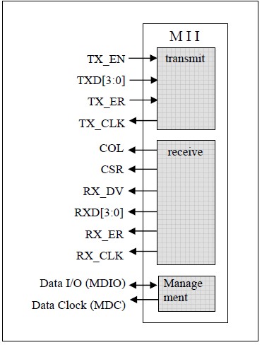
The management interface of the Media-Independent Interface (MII) allows the configuration and control of multiple PHY devices, gathering of status and error information, and the determination of the type and bilities of the attached PHY(s).
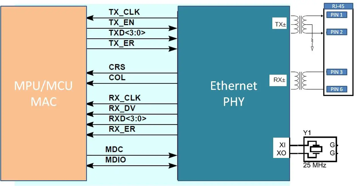
The nibble wide MII data interface consists of a receive bus and a transmit bus each with control signals to facilitate data transfer between the PHY and the upper layer (MAC or repeater). This section provides a simplified block diagram illustrating the connection of a PHY device to an MII MAC interface:
In the Media-Independent Interface (MII) configuration, the PHY generates 2.5/25MHz reference clock on both the TX_CLK and RX_CLK pins. Data transfers between the Ethernet MAC and PHY occur in 4-bit (nibble) groups in each direction, with the Reconciliation sub-layer generating TXD[3:0] and TX_EN signals.
After every group of four data transactions from the MAC sub-layer, the Reconciliation sub-layer utilizes these signals to request the transmission of four data bits on the physical medium or to halt transmission. Clock frequencies vary depending on the Ethernet speed, with 10Mbit/s Ethernet operating at 2.5 MHz and 100Mbit/s Ethernet at 25 MHz, ensuring synchronization and reliable communication between the MAC and PHY.
Media-Independent Interface (MII) Signals
|
Signal Name |
Type |
Descriptions |
|
CRS |
I/O, Z |
CARRIER SENSE: This pin is asserted high to indicate the presence of carrier due to receive or transmit activities in 10BASE-T or 100BASE-X Half Duplex modes. In Repeater or Full Duplex mode, this pin is asserted high to indicate the presence of carrier due only to receive activity. |
|
COL |
I/O, Z |
COLLISION DETECT: Asserted high to indicate detection of collision condition (assertion of CRS due to simultaneous transmit and receive activity) in 10 Mb/s and 100 Mb/s Half Duplex modes. In Full Duplex mode, for 10 Mb/s or 100 Mb/s operation, this signal is always logic 0. There is no heartbeat function during 10 Mb/s full duplex operation. |
|
TX_CLK |
O, Z |
TRANSMIT CLOCK: Transmit clock output from the PHY: 25 MHz nibble transmit clock derived from Clock Generator Module’s (CGM) PLL in 100BASE-TX mode. 2.5 MHz transmit clock in 10BASE-T Nibble mode. 25 MHz transmit clock in 100BASE-T Nibble mode. |
|
TXD[3:0] |
I |
TRANSMIT DATA: Transmit data MII input pins that accept nibble data during normal nibble-wide MII operation at either 2.5 MHz (10BASE-T mode) or 25 MHz (100BASE-X mode). |
|
TX_EN |
I |
TRANSMIT ENABLE: Active high input indicates the presence of valid nibble data on TXD[3:0] for both 100 Mb/s or 10 Mb/s nibble mode |
|
TX_ER |
I |
TRANSMIT ERROR: In 100 Mb/s mode, when this signal is high and TX_EN is active the HALT symbol is substituted for the actual data nibble. |
|
RX_CLK |
O, Z |
RECEIVE CLOCK: Provides the recovered receive clock for different modes of operation: 25 MHz nibble clock in 100 Mb/s mode 2.5 MHz nibble clock in 10 Mb/s nibble mode |
|
RXD[3:0] |
O, Z |
RECEIVE DATA: Nibble wide receives data (synchronous to RX_CLK, 25 MHz for |
|
RX_EN |
I |
RECEIVE ENABLE: Active high enable for receive signals RXD [3:0], RX_CLK, RX_DV |
|
RX_ER |
O, Z |
RECEIVE ERROR: Asserted high to indicate that an invalid symbol has been detected within a received packet in 100 Mb/s mode. |
|
RX_DV |
O, Z |
RECEIVE DATA VALID: Asserted high to indicate that valid data is present on RXD[3:0] for nibble mode. Data is driven on the falling edge of RX_CLK. This pin is not meaningful during Symbol mode. |
Media-Independent Interface (MII) Management Interface Signals
|
Signal Name |
Type |
Descriptions |
|
MDC |
I |
MANAGEMENT DATA CLOCK: Synchronous clock to the MDIO management data input/output serial interface which may be asynchronous to transmit and receive clocks. The maximum clock rate is 2.5 MHz. There is no minimum clock rate. |
|
MDIO |
I/O, Z |
MANAGEMENT DATA I/O: Bi-directional management instruction/data signal that may be sourced by the station management entity or the PHY. This pin requires a 1.5 kW pullup resistor. |
PMD (Physical medium dependent) Interface signals
|
Signal Name |
Type |
Descriptions |
|
TXD+ TXD- |
O |
TRANSMIT DATA: Differential common output driver. This differential output is configurable to either 10BASE-T or 100BASE-TX signaling. |
|
RXD+ RXD- |
O |
RECEIVE DATA: Differential common input buffer. This differential input can be configured to accept either 100BASE-TX or 10BASE-T signaling. |
LED & Reset signals
|
Signal Name |
Type |
Descriptions |
|
LED0/1 |
O |
LEDs (Link/Status/Activity) : Activity Indication LED indicates transmit and receive activity in addition to the status of the Link. The LED is ON when Link is good. The LED blinks when the transmitter or receiver is active. |
|
Reset |
I |
Reset: This pin is an active low reset input. Asserting this pin to active state will force a reset process to occur. Initiation of reset causes strap pins to be re-scanned and resets all the internal registers of the PHY to default value |
Clock Interface signals
|
Signal Name |
Type |
Descriptions |
|
X1 |
I |
CRYSTAL/OSCILLATOR INPUT: This pin is the primary clock reference input for the PHY and must be connected to a 25 MHz 0.005% (50 ppm) clock source. PHY device supports either an external crystal resonator connected across pins X1 and X2, or an external CMOS-level oscillator source connected to pin X1 only.. |
|
X2 |
O |
CRYSTAL/OSCILLATOR OUTPUT PIN: This pin is used in conjunction with the X1 pin to connect to an external 25 MHz crystal resonator device. This pin must be left unconnected if an external CMOS oscillator clock source is utilized. |
Transmit & Receiver Status Signals
The transceiver has two status signals for communications: Transmit Enable (TX_EN) and
Transmit Error (TX_ER). These signals are shown in below Table
|
TX_EN |
TX_ER |
TXD[3:0] |
Description |
|
0 |
0 |
0000 – 1111 |
Interframe gap |
|
0 |
1 |
0000 – 1111 |
Reserve |
|
1 |
0 |
0000 – 1111 |
Send data |
|
1 |
1 |
0000 – 1111 |
Initiate send error |
On the other side, the receive interface has more status signals, as described in below Table
|
RX_EN |
RX_ER |
RXD[3:0] |
Description |
|
0 |
0 |
0000 – 1111 |
Interframe gap |
|
0 |
1 |
0000 – 1111 |
Interframe gap |
|
0 |
1 |
0001 – 1101 |
reserved |
|
0 |
1 |
1110 |
Error of the carrier |
|
0 |
1 |
1111 |
reserved |
|
1 |
0 |
0000 – 1111 |
normal data receive |
|
1 |
1 |
0000 – 1111 |
error receive of data |
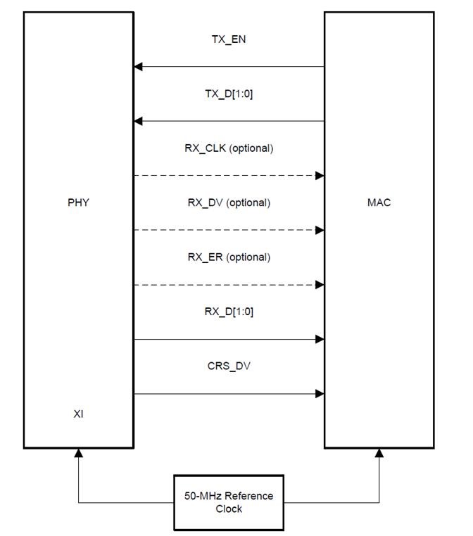
Reduced Media-Independent Interface (RMII)
PHY incorporates the Reduced Media-Independent Interface (RMII) as specified in the Reduced Media-Independent Interface (RMII) specification v1.2. The purpose of this interface is to provide a reduced pin count alternative to the IEEE 802.3 MII as specified in Clause 22. Architecturally, the RMII specification provides an additional reconciliation layer on either side of the MII, but can be implemented in the absence of an MII.
The RMII specification has the following characteristics:
- Supports 100BASE-TX and 10BASE-Te.
- Single clock reference sourced from the MAC to PHY (or from an external source)
- Provides independent 2-bit wide transmit and receive data paths
- Uses CMOS signal levels, the same levels as the MII interface
In this mode, data transfers are two bits for every clock cycle using the internal 50-MHz reference clock for both transmit and receive paths.
|
PINS |
Functions |
|
TX_D[1:0] |
Receive Data Lines |
|
RX_D[1:0] |
Transmit Data Lines |
|
TX_EN |
Receive Control Signal |
|
CRS_DV |
Transmit Control Signal |
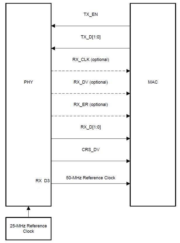
Normally PHYs offers two types of Reduced Media-Independent Interface (RMII) operations: – RMII Slave and RMII Master.
In RMII Master operation, the PHY operates off either a 25-MHz CMOS-level oscillator connected to XI pin or a 25-MHz crystal connected across XI and XO pins. A 50-MHz output clock referenced from PHY can be connected to the MAC.
In RMII Slave operation, PHY operates off of a 50-MHz CMOS-level oscillator connected to the XI pin and shares the same clock as the MAC.
Alternatively, in RMII Slave mode, the PHY can run from 50MHz clock provided by the Host MAC. Data on TX_D[1:0] are latched at the PHY with reference to the clock edges on the XI pin. Data on RX_D[1:0] are latched at the MAC with reference to the same clock edges on the XI pin.
In addition, CRX_DV can be configured as RX_DV signal. It allows a simpler method of recovering received data without the need to separate RX_DV from the CRS_DV indication.
Summary
Media-Independent Interface (MII) Interface Overview
- Standardized method for connecting Ethernet MAC and PHY devices.
- Defined by IEEE 802.3 standard.
- Facilitates communication between MAC (data transmission) and PHY (physical transmission medium).
Features of MII Interface
- Interoperability: Enables seamless communication between MACs and PHYs from different manufacturers.
- Data Transmission: Facilitates reliable transfer of Ethernet frames.
- Flexible Deployment: Allows integration of different PHY devices tailored to specific media types.
- Scalability: Supports various Ethernet speeds (10 Mbps, 100 Mbps, 1000 Mbps).
MII Interface Signals
- Includes CRS, COL, TX_CLK, TXD[3:0], TX_EN, TX_ER, RX_CLK, RXD[3:0], RX_EN, RX_ER, RX_DV.
- Control signals for carrier sense, collision detection, transmit/receive clocks, data transfer, and error detection.
MII Management Interface Signals
- Consists of MDC and MDIO for management data clock and I/O.
- Used for configuration, control, status, and error information gathering.
PMD (Physical Medium Dependent) Interface Signals
- TXD+, TXD-, RXD+, RXD- for transmit and receive data.
- Supports 10BASE-T or 100BASE-TX signaling.
LED & Reset Signals
- Includes LED indicators for link/status/activity.
- Reset pin for initiating reset process.
Clock Interface Signals
- X1 for primary clock reference input.
- X2 for crystal/oscillator output pin.
Transmit & Receiver Status Signals
- TX_EN, TX_ER, RX_EN, RX_ER, RX_DV for transmit and receive control and error indication.
Reduced Media-Independent Interface (RMII)
- Provides reduced pin count alternative to MII.
- Supports 100BASE-TX and 10BASE-Te operations.
- Offers independent 2-bit wide transmit and receive data paths.
- Utilizes CMOS signal levels.
- Operates with a single clock reference sourced from MAC to PHY or external source.
Reduced Media-Independent Interface (RMII) Master & Slave Signaling
- RMII Slave: PHY operates from 50MHz clock provided by Host MAC.
- RMII Master: PHY operates off 25MHz oscillator connected to XI pin or crystal across XI and XO pins.
- Data transfers are two bits per clock cycle using a 50 MHz reference clock.
- These bullet points summarize the key aspects of the MII interface, its signals, and the RMII alternative, highlighting its role in Ethernet communication and network deployment.
Author Profile
- 20+ years embedded hardware design professional with a burning passion for teaching. Sharing the intricate world of embedded hardware is my mission and joy.
Latest entries
 Tech Updates30 November 2025STM32WBA6: The Next-Generation MCU Powering Secure Short-Range Wireless Designs
 Blogs24 November 2025High-Speed PCB Layout Design Guide-104
 Tech Updates14 September 2025Renesas Launches RL78/L23 Ultra-Low-Power MCUs to Power Smarter Home Appliances
 Blogs7 September 2025High-Speed PCB Layout Design Guide-103